Verilog and VHDL Design Hierarchy.
2024.06.16 : I’m Kevin Hubbard, Electrical Engineer. I’ve spent the majority of my 30+ year career designing digital logic circuits in ASICs and FPGAs. It’s been an amazing journey that I hope others will pursue. I’m giving back now in writing this “Getting started with FPGAs” series which starts here.
In Part-6 I explained RTL simulations using the simulator that is included with AMD/Xilinx Vivado tool. In Part-7 I will explain Verilog and VHDL design hierarchy and then how I use my open-source IDE “ChipVault” for managing hierarchy for very large designs.
Unless you are designing a 22V10 PAL ( 10 Flip-Flops ) or maybe even a 7064 CPLD ( 64 Flip-Flops ) – hierarchy and module creation is a very important aspect of digital logic design. Designing a flat design with millions to billions of gates just isn’t feasible. It’s the hardware equivalent of writing an operating system in BASIC with nothing but GOTOs.
Speaking of software, a “module” in RTL ( Verilog or VHDL ) is the hardware equivalent of a “function” in software ( or “method” in OOP ). They are both small blocks that support breaking a big design down into smaller and easier to implement pieces. It’s like that old joke – “How do you eat an elephant? One bite at a time.”
The difference ( and this is a BIG difference ) is that a software function is a chunk of sequential assembly language instructions ( post compiling ) that exists in only one place in main CPU memory ( ignoring cache and multi-cores ). A software engineer can make their code smaller by designing a function and calling it from multiple different places. That function, although used multiple times, never executes at the same time. Early MS-Windows DLLs are rather like that too. They saved a LOT of memory back when memory actually cost something.
With hardware modules, every instance is a unique instance that are all identical. A hardware engineer might design a module for something like a counter. If they use that counter four times in their design, they end up with four counters ( which are 4x the size, or area, of a single counter ). Might seem wasteful, but here’s the thing – those four counters ALL run in parallel ( at the same time ). There’s nothing sequential about digital logic design unless one goes out of their way to make something a shared resource.
What’s a shared hardware resource? Things like a single external DRAM or PCIe interface come to mind. A hardware designer wanting to conserve gates might decide to time-multiplex infrequently used and large resources like a counter or a multiplier. This involves adding muxes and arbitration though.
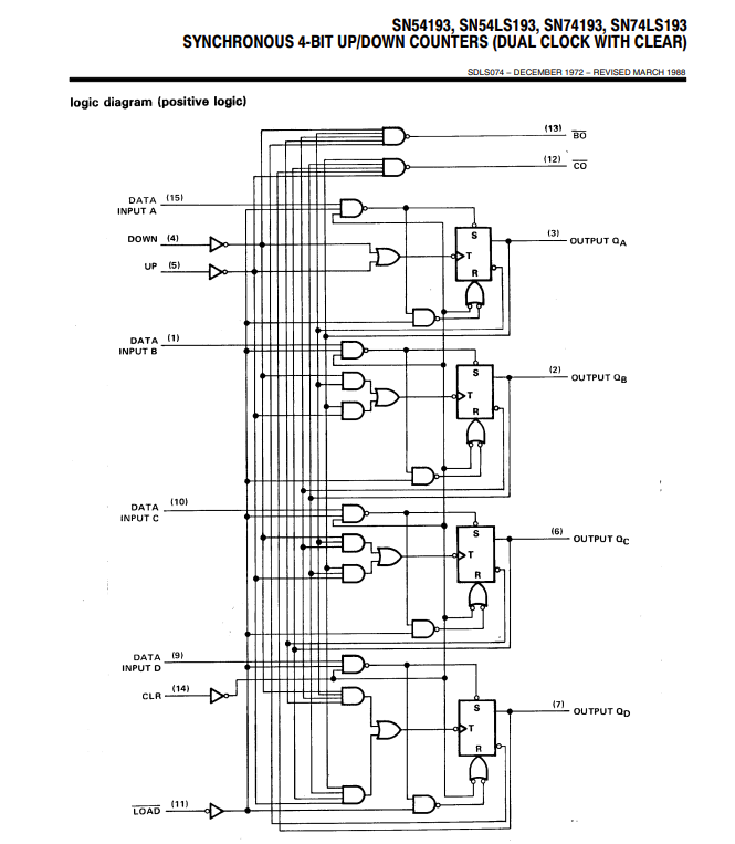
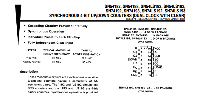
Think of a RTL hardware module like 7400 series DIP IC. The 74LS193 from my 1970’s youth is a perfect example. It’s a 4-bit counter. A board designer could design a PCB and decide to instantiate four of these IC’s on their PCB. They only need to know about the input and output pins ( well, and power and ground ). They don’t need to know the details of the 55 equivalent logic gates that are inside the DIP IC package. They only need to know how it functions at a higher level ( a counter ). When they plop it down on the schematic ( and eventually their PCB ), each “instance” gets a unique name like u0,u1,u2,u3.
Note: You’ll notice in my RTL designs that I carry this u0,etc board designer tradition forward. My RTL instances for “my_74193” get named “u0_my_74193”.
Breaking things down into smaller hierarchical pieces just makes sense.
Let’s look at a Verilog pseudo equivalent to a 74193 as an RTL design module. I’m going to ignore the carry-in and carry-out pins. The 74193 actually has two clock inputs, one for incrementing and one for decrementing. These two clock inputs will be replaced with a single clock and an “inc_en” and “dec_en” ( increment and decrement enables ) control pins. My design is better than an actual 74193 in that you could instantiate it in an FPGA. I’m going to call my Verilog module design “my_74193.v” – it looks like this:
`timescale 1 ns/ 100 ps
`default_nettype none // Strictly enforce all nets to be declared

module my_74193
(
  input  wire       clk,
  input  wire       reset,
  input  wire       load_en,
  input  wire       inc_en,
  input  wire       dec_en,
  input  wire [3:0] din,
  output wire [3:0] dout
);// module my_74193

  reg  [3:0]  my_cnt = 4'd0;

always @ ( posedge clk or posedge reset ) begin
  if ( reset == 1 ) begin
    my_cnt = 4'd0;
  end else begin
    if ( load_en == 1 ) begin
      my_cnt <= din[3:0];
    end else if ( inc_en == 1 ) begin
      my_cnt <= my_cnt[3:0] + 1;
    end else if ( dec_en == 1 ) begin
      my_cnt <= my_cnt[3:0] - 1;
    end
  end
end
  assign dout = my_cnt[3:0];

endmodule // my_74193.v
`default_nettype wire // enable default for any ext IP needing it
I’m very much RTL bilingual, so here’s the identical design in VHDL “my_74193.vhd”:
LIBRARY ieee;
USE ieee.std_logic_1164.all;
USE ieee.std_logic_arith.all;
USE ieee.std_logic_unsigned.all;
LIBRARY std;

entity my_74193 is
port
(
  clk     : in  std_logic;
  reset   : in  std_logic;
  load_en : in  std_logic;
  inc_en  : in  std_logic;
  dec_en  : in  std_logic;
  din     : in  std_logic_vector( 3 downto 0 );
  dout    : out std_logic_vector( 3 downto 0 )
);
end my_74193;

architecture rtl of my_74193 is

  signal my_cnt : std_logic_vector(3 downto 0 ) := "0000";

begin

process ( clk, reset )
begin
  if ( reset = '1' ) then
    my_cnt <= "0000";
  elsif ( clk'event and clk = '1' ) then
    if    ( load_en = '1' ) then
      my_cnt <= din(3 downto 0);
    elsif ( inc_en  = '1' ) then
      my_cnt <= my_cnt(3 downto 0) + '1';
    elsif ( dec_en  = '1' ) then
      my_cnt <= my_cnt(3 downto 0) - '1';
    end if;
  end if;
end process;
  dout <= my_cnt(3 downto 0);

end rtl;-- my_74193.vhd
Now we need to instantiate this module. To make things interesting, I’ll instantiate it twice with one instance counting up while the other counts down. Note that if I just instantiated two up counters and their inputs were all the same, the mapping tool would likely detect the equivalent circuitry and replace the two RTL instances with a single gate-level representation. That’s a useful feature for minimizing the total gate count of a design. The mapper may also do the opposite, replacing a single instance with two if that somehow makes routing and/or timing closure easier. EDA tools have become really advanced over the decades. I’d attempt to explain “register retiming” – but I’ll save that for another day. It’s mind blowing.
Here is “core.v” in Verilog which instantiates two counter instances:
`timescale 1 ns/ 100 ps
`default_nettype none // Strictly enforce all nets to be declared

module core
(
  input  wire        clk,
  input  wire        reset,
  output wire [3:0]  up_cnt,
  output wire [3:0]  down_cnt
);// module core

  reg  [2:0]  enable_sr  = 3'b000;
  wire        enable_loc;
  wire [1:0]  inc_en = 2'b01;
  wire [1:0]  dec_en = 2'b10;
  wire [7:0]  cnt_loc;


//---------------------------------------------------------
// Synchronous enable well after asynch reset.
//---------------------------------------------------------
always @ ( posedge clk or posedge reset ) begin
  if ( reset == 1 ) begin
    enable_sr <= 3'b000;
  end else begin
    enable_sr <= { enable_sr[1:0], 1'b1 };
  end
end
  assign enable_loc = enable_sr[2];


//---------------------------------------------------------
// Instantiate two nibble counters
//---------------------------------------------------------
genvar i1;
generate
for ( i1=0; i1<=1; i1=i1+1 ) begin: gen_i1
 my_74193 u_my_74193
 (
   .clk     ( clk                     ),
   .reset   ( reset                   ),
   .load_en ( 1'b0                    ),
   .din     ( 4'd0                    ),
   .inc_en  ( inc_en[i1] & enable_loc ),
   .dec_en  ( dec_en[i1] & enable_loc ),
   .dout    ( cnt_loc[i1*4+3:i1*4+0]  )
 );// my_74193
end
endgenerate
  assign up_cnt   = cnt_loc[3:0];
  assign down_cnt = cnt_loc[7:4];


endmodule // core.v
`default_nettype wire // enable default for any 3rd party IP needing it
I got a little fancy and used Verilog’s “generate” feature and a for-loop to make two instances without actually typing it twice. Alternatively, it could look like this instead:
my_74193 u0_my_74193
(
  .clk     ( clk                     ),
  .reset   ( reset                   ),
  .load_en ( 1'b0                    ),
  .din     ( 4'd0                    ),
  .inc_en  ( inc_en[0] & enable_loc  ),
  .dec_en  ( dec_en[0] & enable_loc  ),
  .dout    ( cnt_loc[3:0]            )
);// my_74193

my_74193 u1_my_74193
(
  .clk     ( clk                     ),
  .reset   ( reset                   ),
  .load_en ( 1'b0                    ),
  .din     ( 4'd0                    ),
  .inc_en  ( inc_en[1] & enable_loc  ),
  .dec_en  ( dec_en[1] & enable_loc  ),
  .dout    ( cnt_loc[7:4]            )
);// my_74193
Generates are very powerful when combined with parameters as you can decide at “build time” ( meaning Synthesis + Map + Place and Route ) whether to include a module or not. During development for example you might choose to include debugging test logic ( Sump3 ILA for example ) and then remove it for production build. You can also pass in numeric parameters to have certain instances be built differently. My “sump3_rle_pod.v” available here on GitHub is a perfect example of that. Input parameters (constants) decide at build time the width and depth of SRAM to infer.
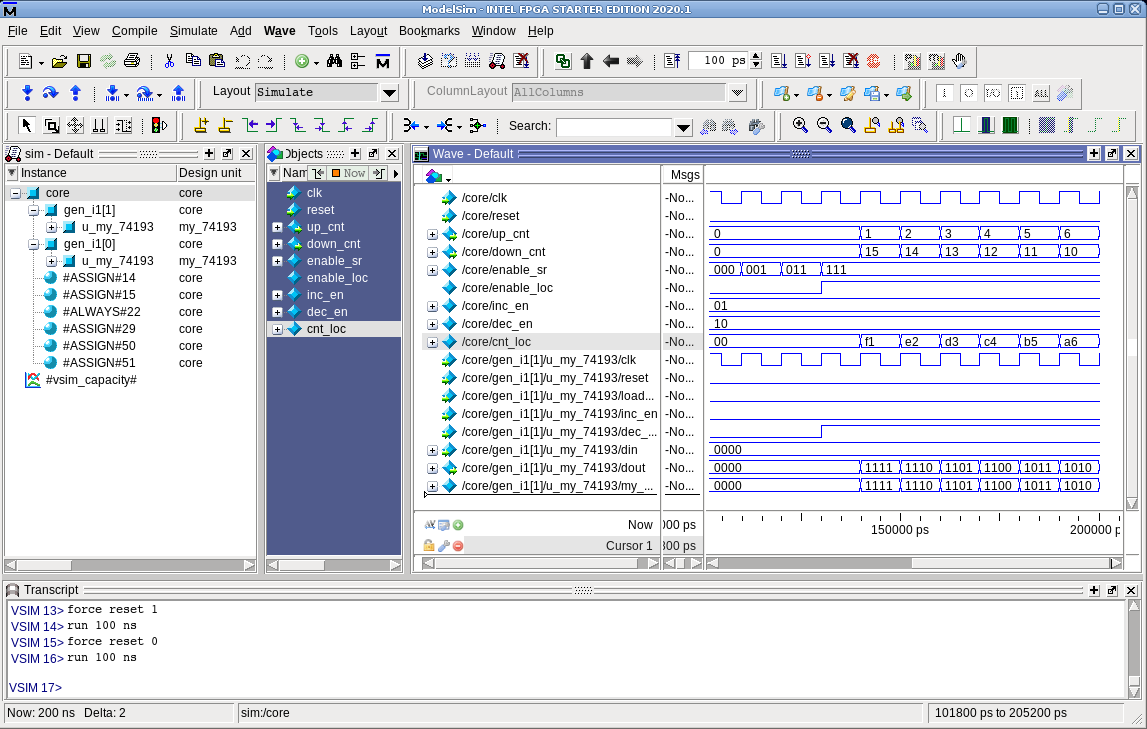
Simulating the design at the “core.v” level shows the two counters running in opposite directions. Note that ModelSim shows the design hierarchy in an expandable/collapsable tree format on the left. Remember this for later.
The VHDL module instantiation looks slightly different:
LIBRARY ieee ;
USE ieee.std_logic_1164.all;
USE ieee.std_logic_arith.all;
USE ieee.std_logic_unsigned.all;
LIBRARY std ;

entity core is
port
(
  clk      : in  std_logic;
  reset    : in  std_logic;
  up_cnt   : out std_logic_vector( 3 downto 0 );
  down_cnt : out std_logic_vector( 3 downto 0 )
);
end core;

architecture rtl of core is

component my_74193
port
(
  clk        :  in std_logic;
  reset      :  in std_logic;
  load_en    :  in std_logic;
  inc_en     :  in std_logic;
  dec_en     :  in std_logic;
  din        :  in std_logic_vector(3 downto 0);
  dout       : out std_logic_vector(3 downto 0)
);
end component ; -- my_74193

  signal enable_sr   : std_logic_vector(2 downto 0) := "000";
  signal enable_loc  : std_logic;
  signal inc_en      : std_logic_vector(1 downto 0) := "01";
  signal dec_en      : std_logic_vector(1 downto 0) := "10";
  signal cnt_loc     : std_logic_vector(7 downto 0);

begin

process ( clk, reset )
begin
  if ( reset = '1' ) then
    enable_sr <= "000";
  else
    enable_sr <= enable_sr(1 downto 0) & '1';
  end if;
end process;
  enable_loc <= enable_sr(2);


u0_my_74193 : my_74193
port map
(
  clk        => clk,
  reset      => reset,
  load_en    => '0',
  inc_en     => inc_en(0),
  dec_en     => dec_en(0),
  din        => X"0",
  dout       => cnt_loc(3 downto 0)
);

u1_my_74193 : my_74193
port map
(
  clk        => clk,
  reset      => reset,
  load_en    => '0',
  inc_en     => inc_en(1),
  dec_en     => dec_en(1),
  din        => X"0",
  dout       => cnt_loc(7 downto 4)
);
  up_cnt   <= cnt_loc(3 downto 0);
  down_cnt <= cnt_loc(7 downto 4);


end rtl;-- core.vhd
Notice that I had to declare the component “my_74193” at the top before I instantiated it. I have two main gripes against VHDL. One is having to type “(3 downto 0)” when in Verilog “[3:0]” is perfectly concise and easier to read. The second is having to declare the ports for any and all modules that a module will instantiate. The tools ( synthesis or simulator compiler ) can easily find the port definitions from the module itself. Packages exist, but they introduce a whole new set of problems.
That ends my quick introduction to designing modules and instantiating them to make a hierarchical design. Managing that hierarchy can be a task in itself.
Way back in 2001 while designing relatively small designs at 250nm I saw the upcoming file and hierarchy management problem. Moore’s Law was doubling the gate counts of ASICs and FPGAs every two years or so. Designs of the future wouldn’t be just a few dozen files ( modules ) of one or two levels of hierarchy depth. No, the writing was on the wall that very soon designs would be hundreds if not thousands of files of unimaginable depths. I won’t say it scared me, but I definitely wanted to be prepared for that day. In preparation for this day, I decided ( way back in 2001 ) to design an IDE tool to manage this unimaginable future. The tool is called “ChipVault” and it is available here on GitHub.
ChipVault isn’t for everyone. It was designed to run on Solaris UNIX ( these days Linux ) and be a wrapper around a text only editor ( namely Vi or now Vim ). Which is to say, ChipVault won’t run on Windows and won’t work well with a GUI based editor like Emacs. What ChipVault does is manage hierarchy, support multiple users working on the same design while also providing a simple yet powerful revision control system for archiving changes ( allowing one to go back in time if necessary ). Most important – it isn’t a vendor specific tool. It’s fully open-source software that doesn’t care if you’re designing an ASIC for TSMC or an FPGA from one of two ( maybe three ) different vendors. It’s only purpose is to manage your RTL.
To get started with ChipVault you first need to put “cv.pl” in your path. Creating an alias for “cv” to be “perl cv.pl” is helpful. Then launching ChipVault is as easy as typing “cv<enter>”. After that, create an “hlist.txt” ( Hierarchy List ) text file that describes all the files in your design and their hierarchy level. That’s it. Now you can launch ChipVault.
# hlist.txt for ChipVault
verilog_example
  top.v
    core.v
      my_74193.v
vhdl_example
  top.vhd
    core.vhd
      my_74193.vhd
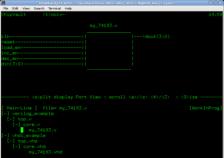
When ChipVault launches, you’ll notice the modules that are parents will have a [+] or [-] next to them. This is the same tree hierarchy view that ModelSim shows. To expand or collapse, just hit the <space bar> key. Using this feature makes it easy to manage thousands of files while limited to a screen of only 50 or so text lines of height. There is no mouse support, all navigation is done with cursor keys. Press <h> for help. Press <q> to quit.
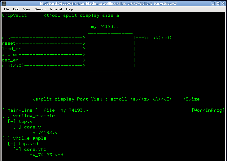
ChipVault can manage ANY text file for you ( not just Verilog and VHDL ). If it recognizes a VHDL or Verilog file, it can optionally render a port view for the module selected with inputs on the left and outputs on the right. This feature may be turned off with the <p> key.
When you want to edit a file, press <TAB> on the file name in main-line. This creates a Work-In-Progress (WIP) version for editing on the right. Only one user can check-out a file at a time and while that file is checked out, other users can see who has it (khubbard in this case). The main-line files are always viewable with <v> key.
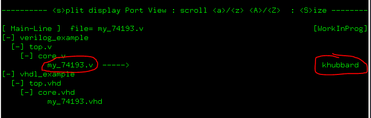
Editing the WIP file is as easy as moving the cursor over it (“khubbard” right of “my_74193.v”) and then pressing <e> to launch the default editor (Vim usually) on the file.
Once editing is done, there are 3 options:
<TAB> : Check the WIP file back in to main-line.
<END> : Perform a UNIX “diff” of the WIP against main-line version.
<DEL> : Delete the WIP file – abandoning all changes made.
A bit of behind the scenes work occurs on the check-in process. It prompts for a change description which then gets appended to a log file ( .history_log.my_74193.v.txt ) and most importantly, it makes a running TAR-Gzip of the current state of the file along with all other previous checkins ( .archive.my_74193.v.tar.gz ). For example, after 100 edits, the .archive.my_74193.v.tar.gz will contain one hundred different versions of my_74193.v. Since they are deltas of each other, the Tarball is highly compressible.
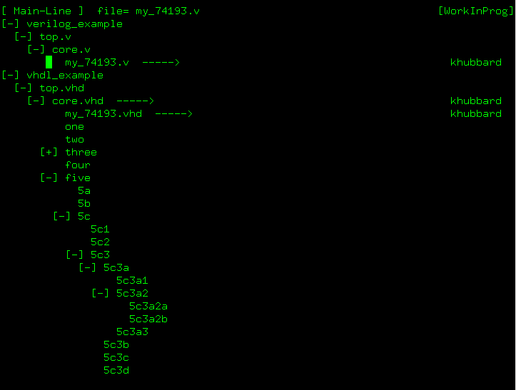
This last screen-shot just shows a fake design with dozens of files that go 9 levels deep in hierarchy. User khubbard has three files checked out for modifications.
And that’s ChipVault. A very simple tool that does a bunch of heavy lifting for managing hundreds to thousands of design files for modern chip designs with millions to billions of gates.
This ends Part-7. In Part-8 I explore Finite State Machines.
EOF

[…] BML FPGA Design Tutorial Part-7ofN […]
LikeLike
[…] BML FPGA Design Tutorial Part-7ofN […]
LikeLike
[…] BML FPGA Design Tutorial Part-7ofN […]
LikeLike