1″ 100W Hot-Plate for SMT Reflow

IMG_1453.JPG

[03.13.2016]

Black Mesa Labs has been using a $20 hot plate for a year now for soldering QFN ICs to PCBs using the BML Inverted Solder Ball reflow technique. This works great for soldering 0.5mm pitch QFN and LGA type packages that would otherwise require messy stencils and paste. Only issue so far has been the size ( 10″x10″x3″ ) and thermal mass of the commercial hot plate as it consumes precious microscope work area and unfortunately stays quite hot for 30+ minutes after a quick 4 minute single IC reflow job.  BML boards are mostly 1″x1″, so a 800W hot plate with a 6″ diameter heating surface is overkill for most jobs.

heating_element.jpg

Wanting something much smaller for a typical BML PCB – stumbled across this 24V DC heating element on Amazon for only $14. It is rated for 24V at 5-7 ohms ( or 4.8Amps ).  A surplus 19.5V DC 5A laptop power brick laying around BML seemed like a perfect match for this element.  BML has safety rules avoiding designs above 48V – so the 100Watt 20V DC supply coupled with the 24V element seemed like a great way to make a lot of heat in a small surface area in a short amount of time.

IMG_1449.JPG

First experiment was to see if this little element would reach +200C in under 4 minutes. Not wanting to cut up the laptop supply’s power connector – located this

71CtDnlyQRL._SL1500_.jpg

power connector adapter for only $5 and cut off the yellow Lenovo end of it and converted it to 0.100″ spaced Dupont connector instead. Hooked up a simple push button switch in line with the circuit – pressed the button and measured surface temperature with a digital thermometer – reached 200C in only 90 seconds!  Too fast for reflowing 40nm FPGAs unfortunately. Wanting to keep the 20V supply – needed to switch to pulse width modulation to slow down the thermal ramp to closely match solder reflow profile of 4 minutes to +200C. A relay? Nah – lets design a custom PCB with power FETs!

pcb.png

After consulting with BML’s “all things analog expert on retainer” DP on how best to switch 100W at 20V – designed a small $2 2-layer PCB as a low-side switch using two IRLML6344TRPBFCT-ND 30V Power MOSFETs in parallel.  Design was drawn ( no schematic ) straight in CopperConnection Gerber drawing tool in less than 15 minutes and fabbed by OSH-Park in about 2 weeks for $2 for a ~1″ x 0.5″ 2-layer 0.8mm PCB.

IMG_1454.JPG

Rds On for this N-FET is 0.029 ohms at 5A ( or  725 mW ) which is near the 1.3W limit for the itty bitty SOT23 device. Not having any heatsinks other than the connection to the PCBs giant “Drain Plane” – opted to share the 5A load across two FETs in parallel. The N-Channel MOSFET’s Source is technically ground – but all the heat is dissipated through the Drain, so large pours on both PCB top and bottom were made to better dissipate the Rds On heat. Design is feed thru for + and – from the supply to the + and – for the load even though the + supply doesn’t touch the circuit at all.  Placed 3 different sized vias 0.125″, 0.079″ and 0.040″ so the board may be easily reused for other projects of various gauge wire needing high voltage and current switching.  A 100K resistor to GND ensures the FETs don’t turn on by themselves without a driver present (powerup Hi-Z) and a 1K series resistor to the Gate of both FETs limits the in-rush current. These Infineon  N-Channel FETs are only $0.29, come in a small SOT-23 package, can switch 5Amps from a 3V LVCMOS signal and are now BML’s go to device for power switching.

20131019_345545.png

Above is a Owon Scope capture of the FET turn on time ( Gate versus Drain ). CH2 ( Yellow ) is the Gate of the N-FET which is driven by LVCMOS 3.3V totem-pole from an AVR through a 1K series resistor. It takes 500ns for the Gate to go from 0V to 1V and then the FET turns on.  CH1 (Red ) is the Drain transitioning from pulled up ( via 1K thru the LED ) to clamping to GND. This transition takes about 2uS total.

10914-01a.jpg


An Arduino Pro (above) was chosen as the PWM controller.  Most BML CPU designs are either RaspPi or Arduino-Zero based ( ARM 32bit ), but BML had this old Sparkfun board in a box and it was the right dimensions as a mechanical base for the project. The 1.5″ diameter heating element is suspended about 1″ in the air, so the wide 2″x2″ Pro board keeps everything from tipping over.
IMG_1451.JPG

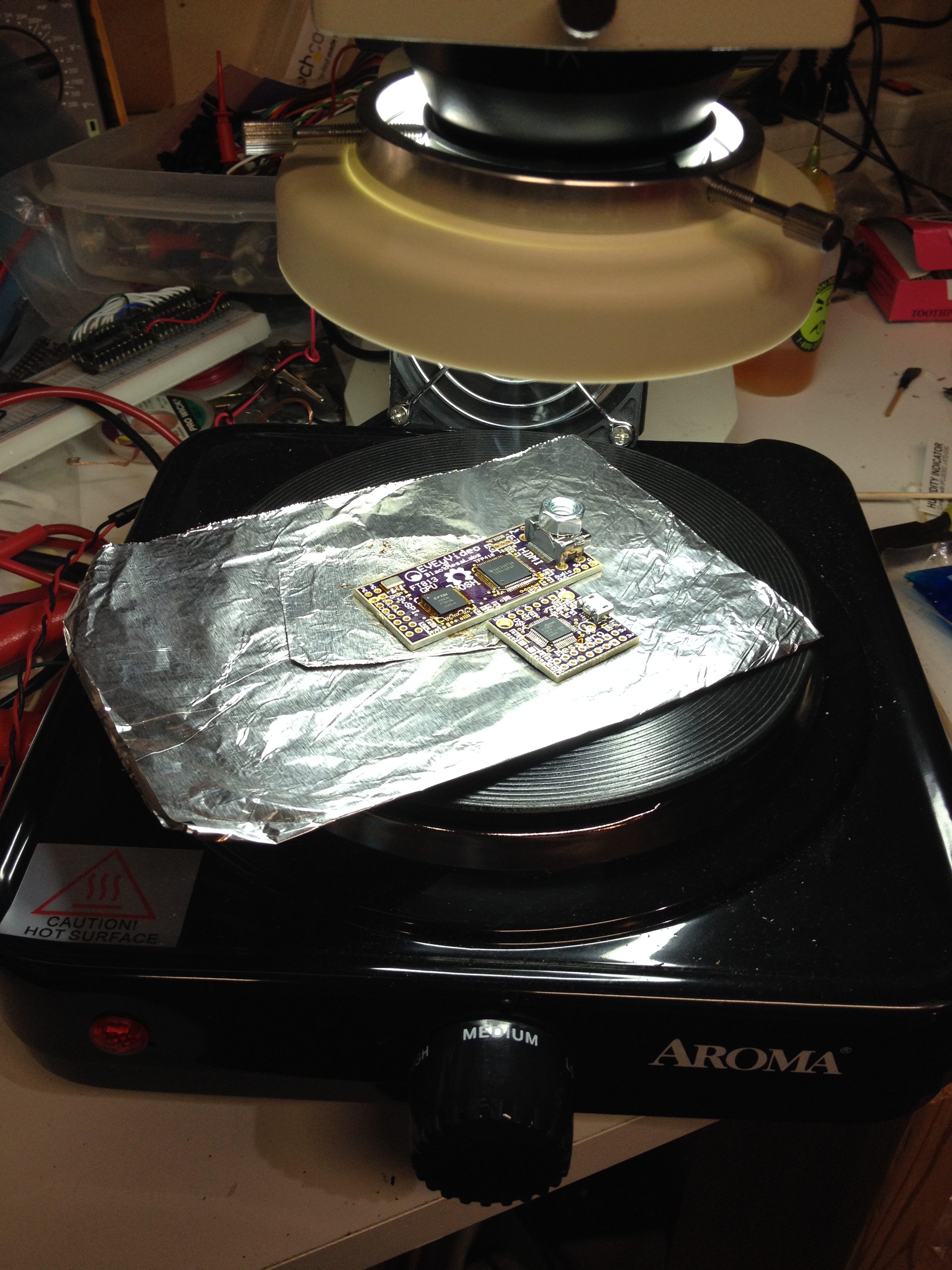
Above picture shows everything cobbled together. A small piece of aluminum foil is wrapped around the element to keep flux from making a mess of it while under reflow. The heating element comes with 22 AWG solid wire crimped to it and extending about 2″ away. The wires are soldered to a 1×2 SIP connector which then mates to another 1×2 SIP connector on the FET board ( being able to remove the heating element from the circuit while under development was VERY important ).  The FET board is placed in the center of the Arduino Pro board atop some poster putty and held in place with the Enable wire (White ), the 1,500 resistor voltage drop network and a ground wire. The Pro can be powered from an FTDI USB cable of course, but to power it from the single Laptop supply, the voltage required dropping down from 20V to around 12V for the on board LDO.  Three 500 ohm leaded resistors each provide about a 2V drop while the AVR CPU is sipping 4mA, for a total drop of around 6V. A large 1K resistor provides 20mA to the red LED whenever the FET gates are turned on and the heating element is getting power.  Total cost was under $20 for the project – not counting the Arduino Pro in the junk box.MLX90614(E,K)SF-xxA.JPG

The Arduino was chosen over an FPGA as the PWM rate is really slow ( seconds ) and the Arduino makes it easy to expand the design and eventually interface to a Infrared Thermometer over I2C via existing tutorials and libraries.  Eventually the design could be expanded to measure the temperature at the surface of the FR4 under reflow for either reporting and / or control.  For now – the dead reckoning PWM method is plenty sufficient.  As the heating element contains very little thermal mass – it cools down in just seconds.

Above is the target solder reflow profile and below is the achieved profile as measured with a thermocouple on a scrap 1″x1″ FR4 PCB.

The GPL’d open source C++ source is available here hot_plate and is fairly straight forward.  When the button is pressed, the AVR starts a 4 minute PWM state machine that gradually increases the PWM duty cycle from 30% to 40% to 60% and then off.  Measuring a scrap piece of FR4 with a thermocouple mounted to it, an ideal reflow profile of 20-150C for 90 seconds, 150-200C for 90 seconds and finally 200-250C for 50 seconds was achieved. Pressing the button mid thermal cycle cancels the cycle. The AVR and giant Pro board is definitely overkill – but the PCB size made it a great platform to mount everything else to.

A word on safety – although this project is under 48V – the amount of heat it can generate could definitely start a fire if powered up in the wrong place ( under a stack of old newspapers for example ) .  To prevent any potential small fires from starting 3 levels of safety were built it. 1) the Arduino runs the heat profile only when the pushbutton is pressed and then automatically turns itself off after the profile time is complete. 2) The 20V 5A power to the electronics goes through a toggle switch. 3) The original laptop barrel connector is quickly and visibly disconnected from the setup when reflow is complete allowing the hotplate to be visibly disconnected from the power supply when not used.

Below is a YouTube video of a Lattice ICE5LP4K-SGN48 FPGA reflowing on the “Mesa Logic DIP” PCB using the BML Inverted Solder Ball reflow technique. This is a general purpose FPGA board on a 0.100″ grid providing 24 user IOs in a 0.600″ x 1.6″ package. This board has a destiny to reach 100,000 feet (~30km) this coming May as a HAB controller for a weather balloon. It will communicate with both an “on balloon” Raspberry Pi and with a ground station via a RockBLOCK Iridium satellite modem using Mesa Bus Protocol. Stay tuned to Black Mesa Labs for an upcoming blog on all the details of the custom HAB electronics.


1″ 100W Hot-Plate for SMT Reflow

The Future is Now!

IMG_1218 - Copy (2)

09.16.2015 – Black Mesa Labs was delivered a very unexpected large 2’x2′ (60×60 cm) package today. BML generally uses a U.S. quarter as a scale reference – but for this – a Pint glass is in order:

IMG_1209

Examining the shipping label – Realized the new Lattice ICE-Ultra FPGAs had arrived 3 weeks early. This new 40nm FPGA from Lattice is a game changer for both BML and the Maker Movement.

IMG_1222

Backstory – Back in May 2015, BML started experimenting with Lattice ICE40 family  as an alternative to large Xilinx TQFP devices for BML designs.  The ICE40LP384-SG32 appeared to be a game changer for BML as it was both low cost ( sub $2 ) and in a 2-layer PCB friendly package ( SG32 ). The big two FPGA vendors ( let’s call them Brand-X and Brand-A ) have gone entirely BGA for their FPGAs – which is completely useless for BML and the OSH-Park style 2-layer Maker Movement PCB designs and assembly. Lattice ( although offering mostly BGA ) has FPGAs in QFN packages ( aka MLFs, SGs ) which can be hand soldered. Sadly – the LP384 proved limited in capabilities – a simple Mesa-Bus bridge design that would easily fit in 200 Xilinx LCELLs completely filled the LP384 as 1/2 the LUTs were used as route-throughs ( consuming limited gates for simple routing ). The LP384 turned out to be about as useful as a large CoolRunner CPLD. But wait….

In June 2015 – Lattice announced that their newer ICE-Ultra ICE5LP4K ( 4,000 Logic Cells ) that was originally BGA only would soon be available in a SG48 package (QFN).  4,000 FPGA Logic Cells for $5 in a 7x7mm package that is 2-layer PCB friendly –  Sign me up!  Fast forward to July – the ICE5LP4K-SG48s were nowhere to be found in normal distribution.  BML contacted both Digikey and Lattice and learned the devices would need to be special ordered in quantity in uncut reels – with a minimum reel count of 50, and a minimum order of 10 reels. The ICE5LP4K FPGAs themselves are only $5, but 10x50x$5= $2,500 – not exactly within BML $100/month beer money budget.  Through persistence and careful negotiations, BML was able to secure a “Special Order” for a single reel of Qty-50 FPGAs – or $250 – manageable. Placed the order in July with an ETA of October 7, 2015 – but they arrived 3 weeks early – Christmas in September!

Inside the giant box was a little LP vinyl sized box and a whole lot of bubble wrap:

IMG_1211

Inside the little box, the giant reel:

IMG_1213

Unfurling the reel – the actual chips – this is all fifty chips:

IMG_1215

Single chip- 4,000 Logic Cells in 7x7mm package for $5 – how cool is that?

IMG_1218 - Copy (2)

Backside you can see how it is 2-layer friendly unlike BGA devices:

IMG_1219 - Copy (2)

This FPGA is really a game changer as it is a true FPGA, much more than just a simple CPLD.  It contains 80 Kbits of SRAM, an on chip ~48MHz oscillator, 39 LVCMOS IOs and 3520 Logic Elements ( LUTS + FlipFlop ). A close Xilinx equivalent ( in a much larger 14x14mm TQFP  package ) would be a device like the Spartan3 XC3S200. This new Lattice device is 1/4 the size and 1/3 the price and 2-layer PCB compatible. 4K LEs aren’t enough for a custom CPU or DSP work – but ample logic for bus bridging, UART designs and complicated FSMs ( Finite State Machines ).  My general rule is 100 LEs a designer can easily consume in a short day of RTL design, 1,000 LEs in a week, 10,000 LEs in a month. 4K LEs is a perfect canvas size for BML designs.

Next up is assembly. BML has 3 PCBs that were waiting for these devices to arrive, Mesa-Video, Mesa-Logic and Mesa-GPIO:

IMG_1221

Initial use for this chip is the Mesa-Bus bridge function – a daisy-chained serial bus that self enumerates based on location in a serial chain and converts clear text ASCII UART serial into either SPI or I2C. Purpose of Mesa-Bus is to provide USB like expansion to simple microcontrollers like Arduinos using only 2 pins ( TXD and RXD UART Serial ). Stay Tuned – the family of Mesa-Modules are about to come alive!

The Future is Now!

“BML Inverted Solder Ball Reflow” process

01_16_2016 Update:

28-LGA.jpg

BML has reflowed 1/2 a dozen of the original QFN packages for the Lattice ICE5LP4K-SG48 FPGA using a hot plate. The same process has recently been modified for use with a LGA-28 packages as well ( shown above – which have no visible pads once placed on the board ). This enhanced process is more reliable and requires less manual soldering ( ideally none ) after reflow. The original method would sometimes result in a misaligned IC due to flux bubbling and lifting the light 7x7mm IC off the PCB prior to solder reflowing. This new process tacks the IC in place with solder – preventing the issues with flux bubbling and the IC moving.

Improved 2016 BML Inverted Solder Ball Reflow process for QFN and LGA devices:

  • Step-1 : Solder bump the PCB pads only for components to be reflowed.
  • Step-2 : Solder bump the QFN / LGA pads of the IC as well ( apply flux too ).
  • Step-3 : Align components under microscope and tack into place using flux paste.
  • Step-4 : Using soldering iron, heat the corner PCB pads going to IC.
  • Step-5 : Solder the ground lug from behind ( if device has one ).
  • Step-6 : Reflow PCB for 4 1/2 minutes on a hot plate ( Aroma ) .
  • Step-7 : Visually inspect and hand touchup pads using soldering iron.

07_24_201532-VFQFN Exposed Pad

IMG_1118

Black Mesa Labs recently developed a unique and new solder reflow process for soldering 0.5mm pitched QFN packages. The process is called “BML Inverted Solder Ball Reflow”.  Rather than apply paste or individually solder bumping the QFN package ( time consuming and expensive ),  the PCB is instead solder bumped ( quick and essentially free ) using a regular soldering iron and standard rosin core solder. Once the PCB is bumped, the QFN is simply reflowed to the PCB using a hotplate. Proper QFN component alignment prior to reflow is crucial and is made possible using flux paste.

The Black Mesa Lab Inverted Solder Ball Reflow Process:

  •   Step-1 : Solder Bump the PCB pads only for components to be reflowed.
  •   Step-2 :  Align components for reflow and tack into place using flux paste.
  •   Step-3 : Reflow PCB for 5 minutes on a hot plate.
  •   Step-4 : Visual inspection and hand touchup QFN pads using soldering iron.
  •   Step-5 : Hand solder remaining components.

How I got on this path is the need to reflow QFN ( leadless ) packages. Xilinx – my goto FPGA provider has gone completely BGA with all their new devices after Spartan6 (45nm) generation.  BGA devices are great unless you are designing 2-layer and 4-layer PCBs and wanting to reflow at home. Basically, I needed a new FPGA vendor that is more aligned with the Maker Movement – small, inexpensive and easy to assemble FPGAs for 2-layer PCBs. Atmel is an awesome company ( they still sell AVR / Arduino CPUs in DIP packages ! ) profiting immensely from Maker community ( all the Arduinos out there ) – but sadly have no FPGA technology.  I discovered Lattice has a 40nm FPGA family called ICE40 that are small inexpensive FPGAs in QFN32 5x5mm and QFN48 7x7mm packages ( majority are still in BGAs of course ). For $2 – $5 I can buy 400 to 5,000 Logic Cell FPGAs that can be soldered to 2-layer PCBs . Compare this to Xilinx Spartan6 XC6SLX9-TQFP144 at 20x20mm at $15 and you can understand my reasoning to chose Lattice over Xilinx for my Maker designs going forward. The picture below shows my new Lattice design ( all components on top side of PCB, FPGA in center ) versus my last Spartan6 Xilinx design ( top side is nothing but FPGA, bottom side has all the other components ).

Lattice Nano-FPGA versus Xilinx Nano6-FPGA Board:

IMG_1126

Back of the larger Nano6 ( with more IO brought out ). Shows all the components on the back.

IMG_0740

QFNs vs QFPs :

48-VQFNsthdmi002abtr

Regarding QFNs ( leadless ) – they are fantastic small and inexpensive packages with great thermal characteristics and compatible with 2-layer PCBs, but difficult to hand solder compared to QFPs ( leaded ) as there are no leads.  They really want to be reflowed in an oven with paste much like a BGA. I almost purchased a toaster oven for BML but Nathan Seidle at Sparkfun.com wrote this great tutorial on using an electric skillet for reflowing surface mount PCBs instead of an oven.  I have decided to try this path for my own prototyping for a number of reasons. One limitation of the skillet method is only populating one side of PCB with components.  If you have seen my previous designs, you know I like to get 2 square inches of components on a 1 square inch PCB – so this is a definite drawback for me.  On the flip-side ( or NOT as it turns out ) I am wanting to start some designs I could potentially have manufactured and sold through Sparkfun – so going single sided for component placement makes sense. Here is a picture of a single sided Sparkfun PCB getting reflowed:

Hot-Plate-Reflow-1

My new PCB designs – “Mesa Zero” and “EVEy Video” are actually my 3rd assembly using the skillet/hot plate method.  The 1st 2 attempts were small QFN32 Lattice ICE40 FPGA boards. 1st attempt was using actual solder paste.  The paste was very messy to apply and post reflow left microscopic solder balls on the PCB solder mask I needed to carefully inspect and cleanup. The biggest downside of solder paste however is the shelf life of only a couple of weeks ( it dries up ). 2nd attempt was using my new Inverted Solder Ball method, but trying to reflow everything with no hand soldering. The small 0603 components tended to bounce around as the flux paste turned to liquid and started bubbling. Both attempts ~worked~, but required a lot of cleanup and hand soldering cleanup post reflow.

One tricky thing about QFNs ( also known as MLFs ) is the substrate ground slug in the center. For many devices – it is the only ground connection and must be soldered – so I place a 0.125″ hole underneath the slug. Unfortunately, this means no routing underneath the package.  For my Xilinx TQFP designs, I always have top-side 1.2V and 3.3V power “planes” underneath the package ( virtual 4-layer ). For QFNs, this isn’t possible as top-side is a ground slug ( and ground is on the bottom side ).

The most difficult thing about QFNs are the leads – they don’t exist – so you can’t see them from above. To check alignment, I need to angle the PCB from all 4 sides.  My 1st attempts I used Elmer’s Glue to hold the package in place while I checked alignment under a microscope.  This actually worked really well, but then I discovered flux paste, solder flux, but in a paste.  A single product replaced liquid flux and the glue. Now I use the flux paste to hold the QFNs in place while I angle the PCB to check aligment. The paste flux melts prior to the solder and becomes a necessary wetting agent ( surfactant ) to improve the soldering process to the pads. Amazing stuff that works great!

IMG_1122

Here is my new procedure in detail, it involves 5 steps but achieves very good results:

Step-1 ) Decide which components I need to reflow on the hot-plate and using a regular soldering iron, solder and liquid flux to tin the pads for those components. This is my “Bumping” process.

OSH-Park Rendering:

mesa_zero

PCB as delivered from OSH-Park:

IMG_0062

Solder placed on QFN and QFPs pads:

IMG_0064


These pictures are the 2 PCBs before and after I solder the pads. The “Mesa Zero” board is a 32bit ARM Cortex M0+  Arduino Zero clone.  The SAMD21 CPU is only $6 and is equivalent in horse power to a Intel 386 CPU from the 1990s containing 256KBytes of flash and 32K Bytes of SRAM in a 7x7mm TQFP48 package.  I designed the board thinking it had a ground slug, but the device does not – so I did not solder underneath that package. The micro-USB connector has caused me grief soldering by hand in the past as the solder tends to flow inside the connector and obstructs cables from plugging in.

OSH-Park Rendering:

eve

PCB as delivered from OSH-Park:
IMG_0066Solder placed on QFN and QFPs pads:

IMG_0067

The “EVEy Video” board is designed around EVE embedded video with a FTDI FT813 800×600 SVGA GPU in a QFN56 package and a TFP410 in a TQFP64 package for reflow and also a small 5x3mm oscillator. This step-1 of soldering the PCB pads with regular solder is equivalent in function to applying solder paste in a normal production assembly.

Step-2 ) After solder is applied to pads I place the components on the PCB and use this Rosin Paste Flux to keep them from sliding around.  The QFPs aren’t that big of a problem as from a vertical viewpoint, I can tell if the 0.5mm pitch leads are aligned.  The QFNs however require me to turn the PCB at 45 degrees for all 4 sides to see if the leads are aligned and is tricky under a 10x microscope. This flux paste keeps the components from sliding around. One caveat is that the paste quickly turns to liquid above about +85F, so the PCB and room must be below that melting point. This picture shows the paste in four corners of each device ready for reflow:

IMG_1100

Step-3 ) Time for reflow.  For less than $20 I bought this awesome Aroma Hot Plate from Amazon

IMG_1107

61O7sGxbKgL._SL1200_

The solder flux seeps through all the vias and makes a sticky mess of things, so I use a sheet of aluminum foil between my PCBs and the hot plate. My 1st attempt I used the “High” setting and I swear the FR4 almost caught on fire ( certainly discolored the OSH-Park Purple to Brownish ). This go around I used “Medium” and it reflowed from “Off” to “Medium” in about 5 minutes. I actually use the hotplate as my permanent “work area” base for microscope work now. Unfortunately, it takes a good 30 minutes to cool down completely.

Step-4 ) Inspection and touchup:

The TQFP had a few leads needing touchup when I inspected with my dental pick.

IMG_1111

The QFN stayed completely aligned thankfully.  I believe that QFNs reflow much like BGAs and tend to “self align” once the solder has turned molten.

IMG_1112

Here is a link to a great video of a BGA package reflowing on top of solder paste slightly out of alignment and snapping perfectly into place. The entire package floats on these molten spheres of solder and aligns automatically.  I believe I am achieving the same results with my QFNs.

Oscillator did well under reflow and stayed aligned.

IMG_1113

I had to remove a bunch of flux ( using a wooden toothpick ) to fully inspect all of the pads on the QFN.  The QFN I could see some “non-silver” on the sides so I went ahead and soldered by hand all the leads just to be certain. The real leads are underneath and can not be visually inspected, but seeing solder on the sides is assurance there is some connection. Once the package is aligned, hand soldering the side “walls” is easy, it is just a matter of rolling a giant solder ball down each side. Step-4 is about soldering all the leads by hand. Step-4 is only possible if Step-3 succeeds in holding the components in place perfectly aligned – which it did. Note that I use really large 0.25 x 1.75mm pads for the QFN when 0.25×0.50mm would normally work.  This makes for easier cleanup as it provides a large surface area for the excess solder to adhere to. Step-4 cleanup is as easy as dumping flux to an area and running my soldering iron tip across it. The solder magically seeks out and adheres to all non solder masked surfaces. No solder wick required. Flux is great stuff. Here is a Before and After of Step-4 on the QFN:

Before Cleanup Pass:

IMG_1117

After Cleanup Pass:

IMG_1118

After Step-4, nothing but silver.  Step-4 is all about hand soldering and inspection of the difficult components. It is imperative to ensure all the difficult components are properly soldered prior to installing the other components as access to the QFNs and QFPs with an iron becomes much more difficult when all the bypass caps, etc are in place. Previously I would use a lot of solder wick for cleanup, now I tend to just use liquid flux as the excess solder will scramble and adhere to the soldering iron tip so long as the tip is clean. This method requires more cleanup ( alcohol and Q-tips – but they are cheap at 1,000 for $10 ).

Step-5, the final step is soldering all of the small components, 0603 and SOT-23, SOIC8 devices and large connectors by hand. Once they are on and I do a final visual component inspection and alcohol scrub and then solder the large through hole connectors. Presenting the final assembly!

IMG_1123

07_25_2015

Spent some time writing FPGA firmware and trying to bringup EVEyVideo. No valid video out yet. Able to toggle the FT813’s GPIO PowerDown output pin, so basic SPI communication is working. Video timing is complicated and this chip has a million registers and proper sequences to follow, so need to persist at it.

07_26_2015

EVEyVideo is Alive!

This morning I succeeded in getting a valid HDMI video signal at 800×600 @ 30 MHz dot clock out of EVEyVideo design. The “@ A B C” are the 1st things I got the GPU to display ( graphics come next ). To save engineering time, rather than try and bring up the FT813 GPU from the SPI Master interface on an Arduino ( and suffer through multiple compile and firmware loading ), I instead created a Nano3 ( Spartan3 XC3S200A ) FPGA design that provides 16 GPIO pins on the Nano Bus header.  This FPGA design can be re-used for anything as all 16 pins are configurable for Input,Output, Drive-1-Only or Drive-0-Only. Having a software bit-bang interface at 1st means I can script everything and iterate rapidly. Here is my 1st image:IMG_1129

Note: About the Nano Bus.  The “Nano Bus” isn’t actually a bus, but an electrical interconnect standard I established at BML for all of my FPGA and peripheral designs.  If you are familiar with PMOD, it is similar, but I think better of course. “Nano Bus” provides 2 GND pins, 5V Unregulated Raw Power ( current limited at 3A by pin ) and 3V regulated ( limited current by masters LDO ). The connectors are color coded Yellow=5V, Red=3V and Green = GND. I can quickly spot 2 PCBs with the Yellow and Green identifiers and know that I can plug them in without blowing anything up. The remaining pins, typically 4,8 or 16 in a dual row configuration are digital IO pins at 3V.  I have splitters that convert a x16 master to two x8s, or a x8 and two x4s, etc.  Also have “Gender Benders” so that I can plug 2 Masters together ( an FPGA and an Arduino for example ). It is a cost effective and versatile interface as I can build a FPGA with a x16 ( 2×10 0.100″ ) Nano Bus Header and plug a small x4 SPI peripheral board into it that is only 1/2″ wide. OSH-Park charges by the square inch, so I can build Nano Bus SPI chip peripherals boards for only $2-$3  that have a 2×4 0.100″ connector ( 2 GNDs, 5V,3V and 4 signals ).

Back to EVEyVideo bringup, so with the Nano3 FPGA as SPI Master to the FT813 in place, I then wrote a Python script for bitbanging the SPI Bits over a standard FTDI USB serial cable. Every SPI clock cycle takes two FTDI serial port writes at 921,600 baud which is REALLY slow of course ( takes about 1 minute for FT813 bringup ). Using this flow means I avoided compiling Arduino C code and flashing firmware. Scripting languages like Python, Perl and Powershell are a tremendous time saver for initial hardware bringup. C is king for final performance but awful for iterating and trying things.

That ends this blog, the EVEyVideo board is fully assembled and electrically all tested out. I will start a new blog in the future specific to EVEyVideo programming and where I plan to take this OSH project. My end goal is to provide a low cost and easy to use video interface for Arduino developers.

“BML Inverted Solder Ball Reflow” process

USB 2.0 FTDI 12Mbps Serial Converter Board Assembly

IMG_0820

[ 01.12.2015 ] Assembled my new USB 2.0 12Mbps UART board today.  Thought I would take the opportunity to blog about the entire process from start to finish – board design, procurement, surface mount assembly and final test.

imgres

[ 12.23.2014 ] Started new ExpressPCB 2-layer design for a small 1″x0.5″ board to replace a standard 1Mbps FTDI Cable but run 12x faster using a USB 2.0 chip from FTDI – the FT232H.  All of my previous FTDI board designs have used the FT232R as it is a smaller chip that includes an oscillator and all the USB passives on chip.  The FT232R interfaces to USB at a conservative 12 Mbps versus SERDES 480 Mbps for the FT232H.  The FT232H requires a lot more support circuitry ( 12 MHz precision oscillator, protection diodes and is in a bigger package ).  Expecting a 2-layer PCB to work at 480 Mbps was a huge $3 gamble I was willing to take.

express_pcb

[ 12.26.2014 ] Finished the design ( working on it part time – had other things going on the last few days ). Typical design flow is schematic design and then have a computer autoroute. My flow is quite different in that I manually place components where I think they can be routed using only two layers and also assembled by hand in as small area as possible. Using ExpressPCB version 7.0.2 (only), layout is done manually using a vector drawing program.  Red signifies copper on the top, green copper on the bottom, yellow silkscreen on top for labeling. Designing a PCB like this is very much a challenging puzzle.  After I finish the design, I import the ExpressPCB file into CopperConnection and export a single *.ZIP containing layer Gerbers and Excellon drill files in OSH-Park selected format. This process takes about 10 seconds. I could actually layout my board design in CopperConnection – but I already know ExpressPCB  – so why bother learning a new tool? ExpressPCB is a great service for at work when I need a board fast. When I’m not in much of a hurry, OSH-Park is super inexpensive and high quality.

copper_connection

[ 12.26.2014 ] Uploaded Gerber and Excellon *.ZIP file of design to OSH-Park. The website takes a few minutes and presents a rendering of all the different layers ( Copper, Solder Mask, Silkscreen, Drill holes ). Approve and purchase the design 0.61×1.21 inch (15.39×30.66 mm) 2 layer board for $3.65

osh_parktop_copperbottom_coppertop_silkscreentop_soldermaskbottom_soldermaskexcellon_drills

Here is an example OSH-Park panel that I found on the web that they showed at a Makerfaire in Portland in 2013. Notice how small all the designs are and how much daylight shines through. Their software does a fantastic job of panelizing multiple small gerber designs. Other low cost PCB places like IteadStudio stick with simple fixed rectangles on a 5x5cm grid and charge on those dimensions even if your design is much smaller. I often look at other people’s OSH-Park designs at flickr site to see how far they stretch the 2 layer and 4 layer capabilities.

osh_park_panel

[ 01.10.2015 ]  Bare boards arrive in the mail. They usually have rough snap-off edges which are easily filed down with a metal file.

IMG_0821

[ 01.12.2015 ] Surface Mount Assembly begins.  My tools are a 10x/30x microscope, a Weller-Ungar 921ZX soldering station with a screwdriver tip, GC Electronics Liquid solder-flux 10-4202, Kester “44 Rosin Core” lead solder 66/44 0.5mm .020″, Chem-Wik 0.075″ solder wick,  Isopropyl Alcohol 99.8% IPA, Cotton Swabs, Dental Pick, Tweezer and “Dexter” leather gloves. I also have a 4″ surplus case fan at the back of my microscope to take away the fumes.

IMG_0823

I always start by placing the QFP 1st as alignment is crucial with 0.5mm pitch between pins. Once the package is perfectly aligned ( 10x magnification ) I pour solder flux liberally along the perimeter. Flux is amazing stuff, not only does it perform Jedi mind control on molten lead to seek out copper and avoid solder mask – but it is wonderfully sticky stuff and does a fairly decent job of keeping the QFP from drifting out of alignment.  That said – I always tack down the corners first with just a bit of solder and then pour the solder on thick – rolling across all the leads. End result – complete ugly mess, shorts everywhere – but the leads are all attached to their pads in perfect alignment.

IMG_0806

Pass-2 ( you knew there had to be a pass-2, right ? ) – Solder Cleanup.  The wick combined with the flux on the board magically sucks up the excess solder shorting all the leads.  This step gets really hot really fast. I protect myself ( finger tips ) with my Dexter gloves ( thin unlined leather ) so I can position the wick and not burn myself.  I protect the chip by only wicking about 4 pins at a time then pull back and let the IC cool down for a few seconds before proceeding.  Takes patience but perfectly soldering an internally fried chip to a board is a real bummer. I do own a nice hot air reflow station where I can remove bad ICs -but I generally would rather just start a new board assembly from scratch than rework a bad one.

IMG_0807

Pass-3 : This pass is optional, but is worth the effort.  Apply lots of IPA ( the kind that makes you go blind – not the tasty beer ) and cotton swab scrubbing to remove all the flux.

IMG_0808

Pass-4 : With the QFP clean, I crank my microscope up from 10x to 30x and go around to each pin with a dental pick and check for bad solder joints ( loose pins ) or any shorts. I usually don’t find any, but the time to check is before all the other components are soldered to the board as access to the QFP pins becomes difficult if there are other components around.

IMG_0824

Once the QFP is on everything else is pretty straight forward.  I only use 0603 for Bypass caps ( 0.1uF ) and 0805 10uF Bulk Caps and 0805 resistors.  This speeds up assembly as I don’t need to look up each component in the design file, I can tell just by the pad size and what its connected to determine what to place.  For example – I never connect a 0805 resistor between power and ground – so it must be a 10uF bulk cap.  For the small SMT 0603s and 0805s I drop a bit of solder on 1 of 2 pads, then apply to component with tweezer and resolder the 1st pad to the component, then with the component firmly ( fully planar ) attached to the board, I apply solder and the iron tip to the 2nd pad. After this, the 1st pad usually needs some more solder to make a good looking connection.  Thats it – I’m done with assembly!

IMG_0820

Before test – I take a moment to reflect and decide what I would do differently to make assembly easier in the future.  For this design the microUSB connector was a problem. It is designed for solder paste and oven reflow assembly as the leads are recessed behind the shield housing.  I was able to solder them eventually, but a little more space between the connector and QFP would have been better. Mini-USB is MUCH easier to hand solder. Another issue I discovered is the shield extending behind the leads unexpectedly results in the shield resting above my 5V trace on the top side.  The solder mask is the only insulation preventing a short from 5V to shield return.  Prior to plugging into my computer, I applied my 5V DC supply to 5V PCB rail and the shield and confirmed no short.  This is OK for a one-off, but I immediately created a new “fixed” version of this design and moved the 5V trace south about 0.010″ to clear the shield. For $3.50 I will probably fab out this “fixed” version and scrap the remaining 2 unstuffed PCBs of Gen-1 if  I decide I need more than 1 unit.  The micro USB connector was the only issue, so moving on….

Time for test. Plug and pray a micro USB cable from my computer into the board.  And look at that! COM5 ready for use.

IMG_0813IMG_0811

1st test is to send 9,600 baud to my scope. Bit length is about 100us, or roughly 10,000 Baud.

IMG_0812

2nd test to send 921,600 baud to my scope. Now the bit length is about 1us, or roughly 1Mbaud.

IMG_0814

3rd and final test, run my Powershell  script that talks directly to FTDI device driver DLL and configure port for 12Mbaud.

IMG_0815

Excellent! I’m in business.  I now have a USB 2.0 to 12Mbps UART serial interface into my FPGA designs that is electrically and mechanically compatible with my existing FPGA boards ( that are designed for the industry standard FTDI cable ).  That ends my Black Mesa activity for tonight.  Next tasks are to change my FPGA design for the faster baud rate ( simple divisor setting in Verilog ) and establish Backdoor communications (Register Reads and Writes using BD_SHELL.exe ) and then time SUMP.exe data dumps from FPGA to computer and compare date rates between 1Mbps cable and 12Mbps board. Due to Windows and Powershell limitations – it may or may not be faster.  If it is faster ( like 10x faster ) – my next iteration of the design is ready to be assembled. This uses the same chip, but interfaces using 16 wires over a Nano x16 header instead of the FTDI 2 wire 1×6 connector. Spec says transfer rates should be 40 MBytes/Sec ( 320 Mbps ) – which theoretically would be 27x faster than my existing design that is already 12x faster than my existing FTDI cable. That project is for another day however.

i

USB 2.0 FTDI 12Mbps Serial Converter Board Assembly