Modelsim VHDL+Verilog Install Tutorial

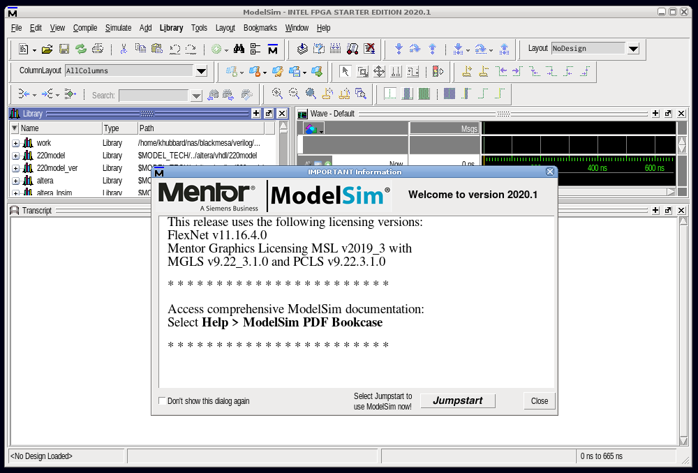
2024.04.21 : Intel currently ( 2024 ) makes the ModelSim Questa “Intel® FPGA Starter Edition SW-QUESTA” free to use – which is pretty fantastic. Will this fantastic EDA tool deal continue as Altera gets spun-off as a standalone company from Intel? I have no idea – but I do think it’s a great time to install “SW-QUESTA” on my home Linux and Windows machines. I like to write VHDL and Verilog RTL just for fun – so here’s a quick tutorial on how you can too!

[ Downloading the Software for Linux / Windows from Intel ]
For Linux, “Razer6” has a great writeup here on GitHub for an Ubuntu installation. The only complication was the need to install some old 32bit packages using:
sudo dpkg –add-architecture i386
sudo apt-get update
sudo apt-get install libc6:i386 libncurses5:i386 libstdc++6:i386 lib32ncurses6 libxft2 libxft2:i386 libxext6 libxext6:i386

Then run the installer and modify your .bashrc file with:
export PATH=$PATH:/opt/modelsim_ase/bin

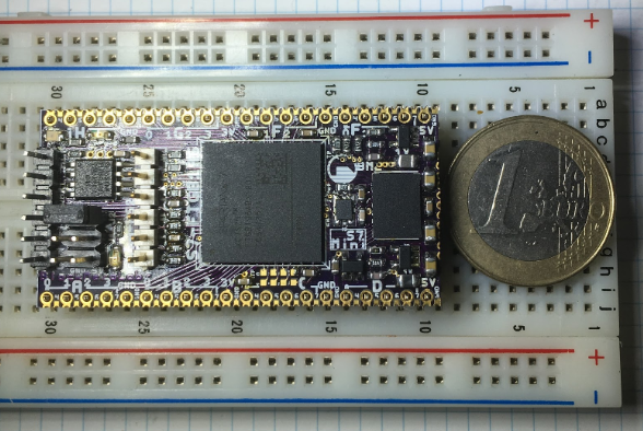
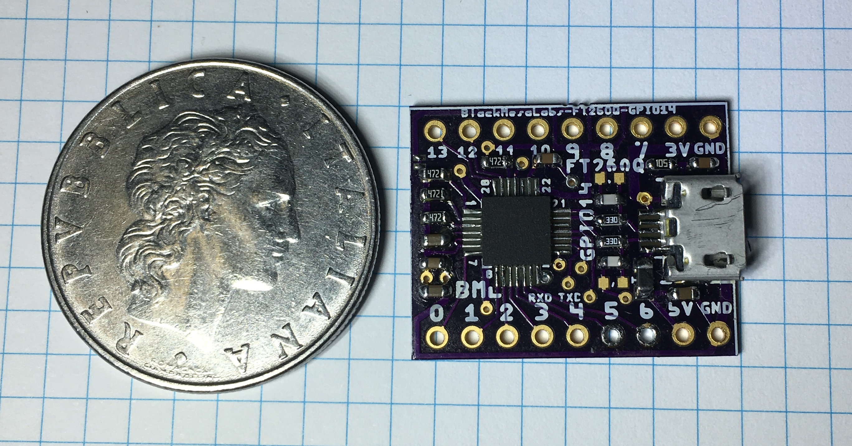
I actually have two Linux workstations at Black Mesa Labs, “GLaDOS” and “Lambda“.
“GLaDOS” is my primary workstation and runs FC19 ( Fedora Core 19 aka Schrödinger’s Cat ) an equivalent to RHEL7. It’s REALLY old ( 2013 ) – but I have Xilinx WebPack ( also free ) installed and running on it for my many BML Spartan3 and Spartan6 FPGA designs, so I keep it around. It’s a great SOP – take old unwanted laptops, slap in a new SSD for $30 or so and install the latest Linux and run it headless in the background with just power and ethernet connection.

“Lambda” is a modern Ubuntu 22.04.3 LTS 64bit installed on a gaming laptop gifted to me recently ( ASUSTek G551JM, Intel Core i&-4710HQ 2.5 GHz x 8, 16 GB DRAM and a 256 GB SSD ). I use “Lambda” when I need to install modern software packages, most recently the “cc65” C compiler for making Apple ][+ programs. I just “ssh -X” into Lambda from GLaDOS and everything – including GUI apps just work. I should mention that even though GLaDOS is my “desktop” Linux workstation – it’s actually headless. I use a NoMachine client from a generic MS-Windows desktop – my actual desktop computer with screens, a keyboard, mouse, speakers, etc.

Anyways – the Ubuntu install on “Lambda” went just fine – although it took at least half an hour. The installer launched on “GLaDOS” no problem, but complained about lack of disk space, requiring 5GB with only 4GB available. It’s a 64 GB SSD from 2013 – so I’m not too surprised or disappointed. “GLaDOS” will need to sunset someday anyways. Computer operating systems age about like dogs do. Way too fast.

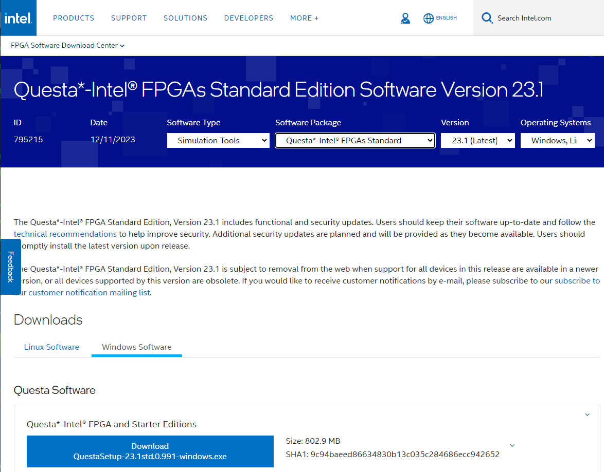
The MS-Windows install was super simple, just downloaded the EXE from the Intel website here. Complications only started with licensing.

[ Licensing ]
For whatever reason – the Linux version doesn’t require a license file and it just runs. How great is that??The MS-Windows version though – it requires a LICENSE.DAT file that is node locked to your PC’s Ethernet MAC address. It was quite the process getting this (free) file. I almost gave up in tears. Story continues…

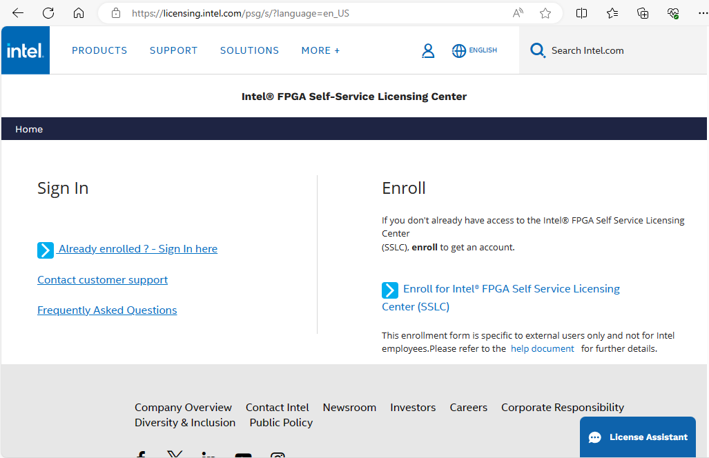
Step-1 : Enroll for Intel FPGA Self Service Licensing Center ( SSLC ) at this link . This was fairly straightforward ( at 1st ) entering my email address and creating a password. Later on I discovered that thanks to browser cookies, you can only do this once. To create an account with my alternate email, I had to use a different (Edge) browser. Why two accounts? I’d like to install this on my work laptop for those times I’m away from the license server ( think on planes, trains and automobiles ).

Step-2 : Login to eventually request a license from here. Things got really strange though. I got stuck in a Microsoft / Intel Azure loop of hell. To request the Intel license, I had to login not using my new Intel account ( my email + password ) but using my existing home MS-Azure account ( email + password ). It wouldn’t let me though. It said I had to configure MFA authentication. The thing is, I only have one cell phone number and it’s tied to my other (not home) MS-Azure account. Now even though I went through Microsoft Azure and configured a 2nd email as my MFA – Intel Azure wouldn’t accept it. It demanded either a cellphone number or an authenticator app. I don’t quite understand Azure.

So I punted. Rather than getting a 2nd cellphone, I researched authenticator apps and downloaded and installed “Google Authenticator” on my existing cell phone and gave that to Intel’s Azure and it got me in ( finally ) to request a license file. TBH – I almost gave up. Now I’m left wondering when I will need to use “Google Authenticator”. When I login to MS Azure here – it still has my backup 2nd email as my MFA – with no mention of “Google Authenticator”. So apparently I only need this for my new Intel account. I really don’t understand Azure.

Step-3 : Collect your MAC ID ( from a DOS box type “ipconfig /ALL” – its the 12 digit hex number for your Ethernet adapter ). Submit and receive a LICENSE.DAT file via email. Now under [ This PC ],[ Properties ], [ Advanced System Settings ],[ Environment Variables ] create a new variable “LM_LICENSE_FILE” and point it to LICENSE.DAT. Again – this step is not necessary for Linux. Strange.

In summary, if you don’t have an Azure account or you do but not willing to share an MFA with Intel – you’re not getting a license file for running ModelSim Questa on MS-Windows. Sorry Charlie.


[ Intel / Altera Customized ]
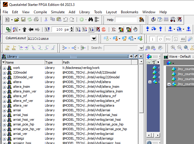
So what is Intel/Altera about this version of ModelSim Questa? It comes pre-bundled with Altera FPGA gate primitive libraries installed and ready to go. It’s a hassle to install these manually, so this version does all the work for you ( which is also why the install is 5 GB ).

[ Compiling your design ]
From the command line ( DOS or Linux shell ) type “vlog foo.v” or “vcom foo.vhd” where foo.* is your Verilog or VHDL RTL file. Note that the compile commands are different. Why exactly? Long ago legacy license reasons I suspect. With large designs with multiple levels of hierarchy, I typically make a “vcom.sh” script to compile everything. Much like nuking LV-426 from orbit – recompiling every single file of a large design is the only way to be sure everything is up to date in the “./work” library.

[ Simulating your design ]
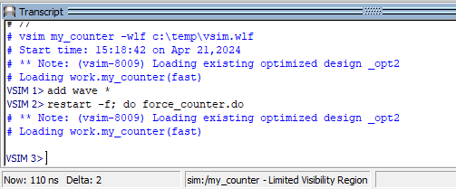
From your OS’s command line ( DOS or Linux shell ) type “vsim foo”

[ Observing your signals ]
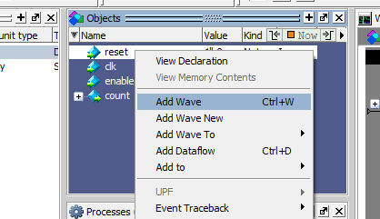
In the “Objects” window, right-click on signal names and select “Add Wave”. Alternatively, from the “Transcript” command line type “add wave *” to view all signals at this hierarchy level. “*” can be replaced with a specific signal name. All of these commands may be scripted up in a “do file” too of course.

[ Simulate your design ]

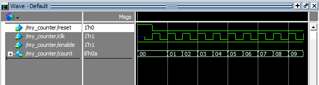
I typically generate “do files” as stimulus that look like this:
force reset 1
force enable 1
force clk 0 5 ns, 1 10 ns -repeat 10 ns
run 10 ns
force reset 0
run 100 ns

and then from the “Transcript” command line type this:
restart -f; do foo.do
Now’s a great time to ask – “Why use ‘do files’ instead of writing a test bench?”. Great question. Test benches – although useful – can also be very deceiving. A person may write a test bench and decide – “well if it passes the test bench then my circuit is golden.” – but that’s absolute bullshit. Does the test bench launch stimulus signals at clock-0 and read the results? Or does it launch at clock +1, +2, +3, +4 etc relative to other stimulus? I’m all for exhaustive test benches with random number generators. I’m all against test benches that test exactly one single scenario out of many possible. “Do Files” allow for rapidly iterating and testing multiple scenarios. I’m all in for that. That’s golden.

[ In Closing ]
All in all this ModelSim Questa “Intel® FPGA Starter Edition SW-QUESTA” install went very well. If it wasn’t for the MS-Windows install requiring the license file from Intel Azure hell – it would have been quite simple. One issue I did have ( both on Windows and Linux ) was the Waveform window only displaying “-No Data-” after a simulation, with no sim results displayed. I tracked this down to a very strange incompatibility between Modelsim and my Synology NAS ( Network ) drive regarding the simulation *.WLF file. I suspect Modelsim does an write-append operation while also reading the same file handle and Synology doesn’t support this and Modelsim appears to read 0 content file. Thankfully I figured out a workaround. I can use the “-wlf” flag for vsim to store the *.WLF file locally. For example:
vsim foo -wlf ~/vsim.wlf ( Linux )
vsim foo -wlf C:\temp\vsim.wlf ( Windows )

Alternatively, modify the modelsim.ini file to look like this:
WLFFilename = /home/khubbard/vsim.wlf

It didn’t like “~/vsim.wlf” for whatever reason. There’s a bunch of WLF flags and there may be one that makes it work just fine writing to Synology NAS. I’ll experiment more in the future.

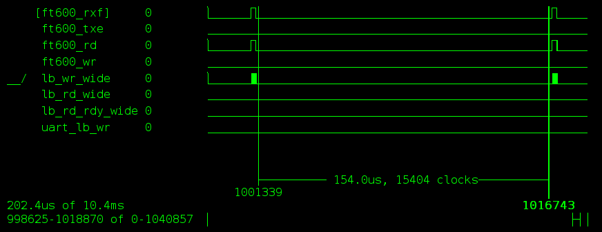
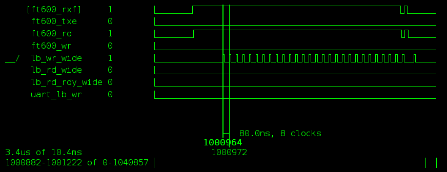
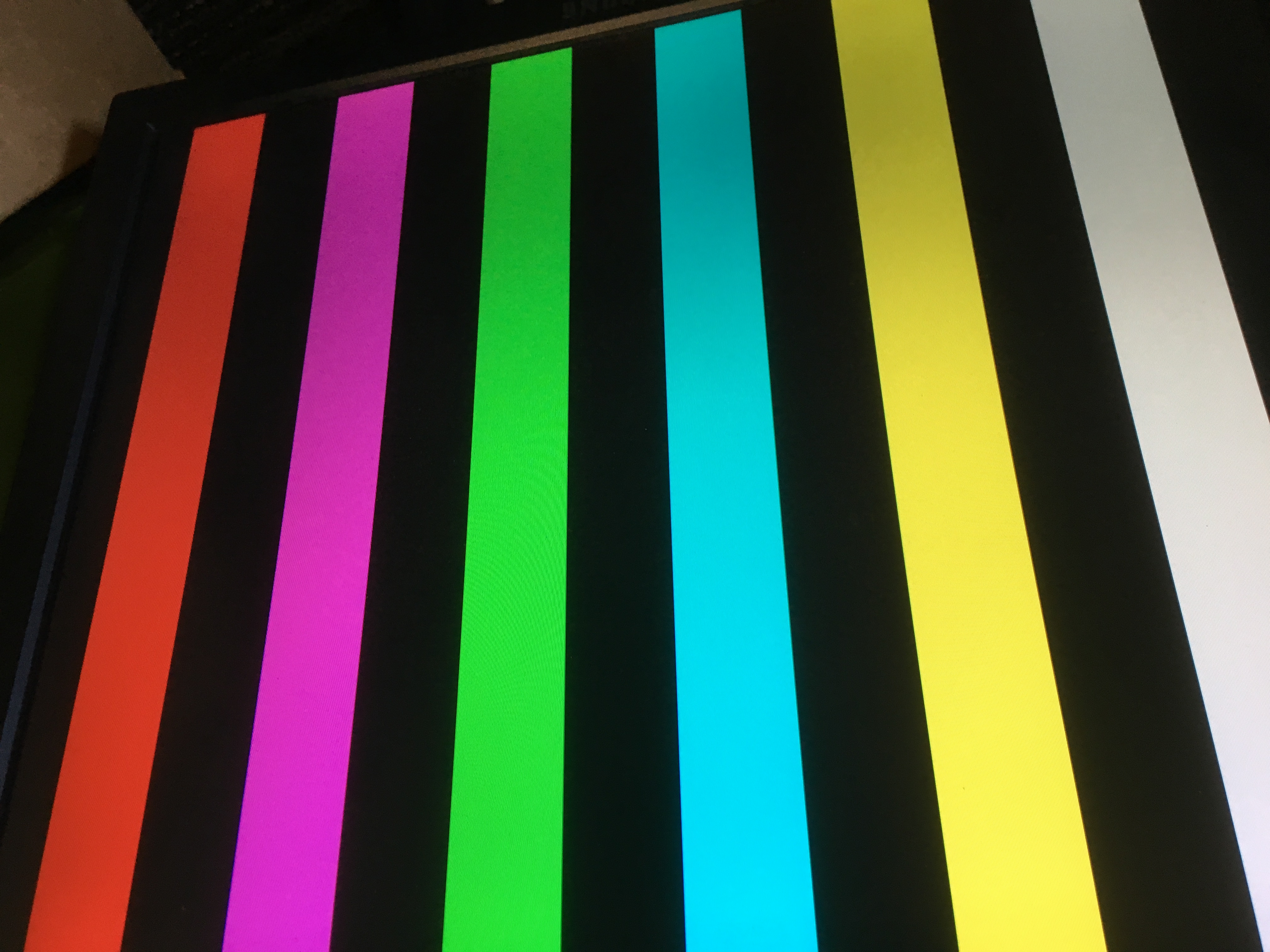
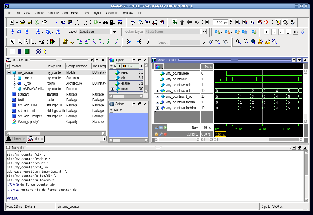
This “Free” version of Modelsim Questa from Intel/Altera is definitely slower and less capable than the commercially licensed version. Reportedly runs at 40% speed of purchased versions. It’s also less expensive – which is great for hobbyists like myself. That said, I was shocked ( pleasantly surprised ) to see it simulate my mixed Verilog and VHDL design below without issue. Years ago that would suck up two simulation licenses and really steered people away from mixed designs for a poor reason.


Having used ModelSim professionally for 30 some years – I’m very excited to be using it at home now too. It’s a great ( the best IMHO ) RTL simulator and I’m excited that more people will be able to use it going forward. Expect to see more detail in future BML blogs on using ModelSim Questa.
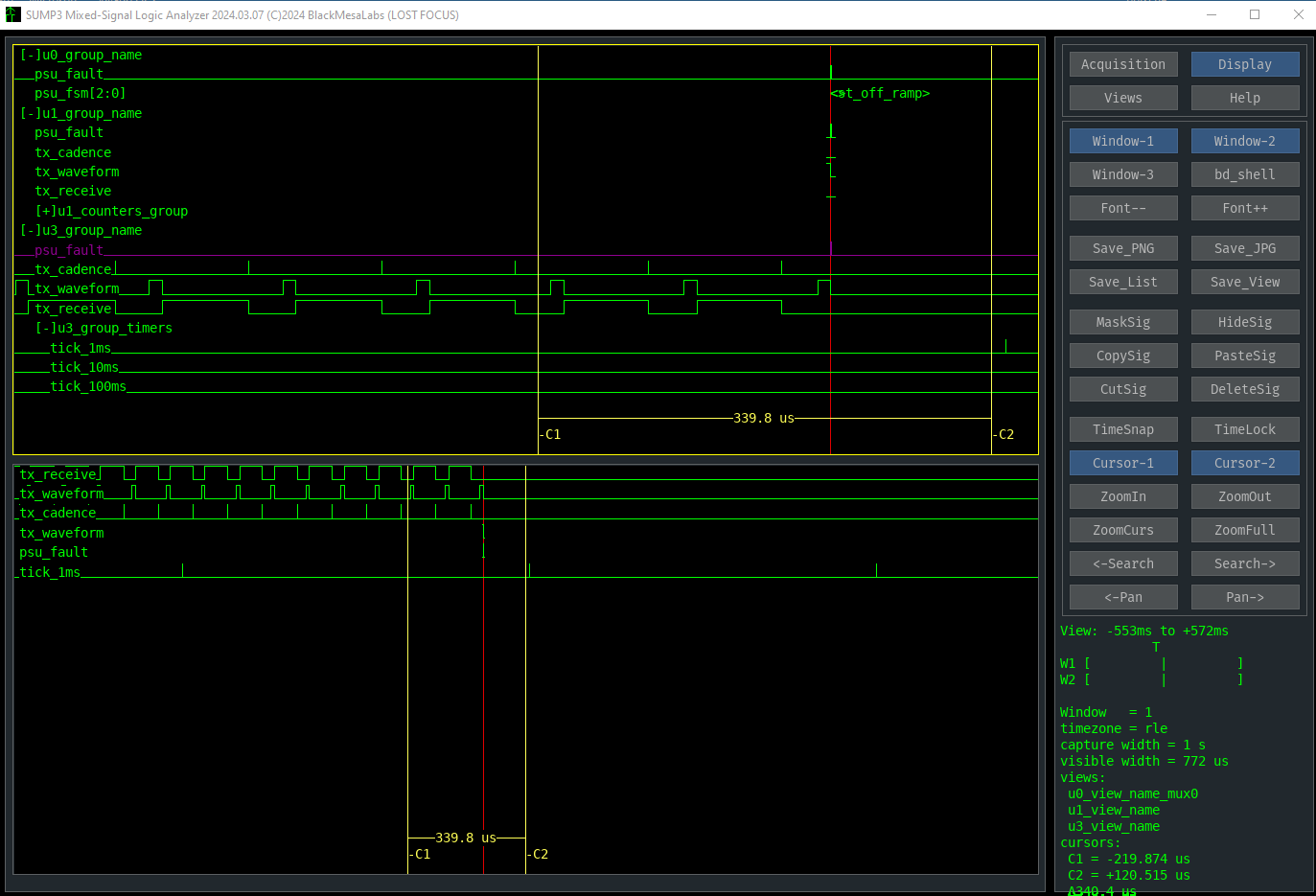
For Example, Come back next time and I’ll discuss test benches and VCD file exports and imports from both ModelSim and the BML Sump3 ILA.

2024.04.27 : Update – I got ModelSim running on my 11 year old Fedora Core 19 Linux workstation. Took a lot of Googling and “yum install” trial and errors to get all the libraries needed.
yum –enablerepo=fedora clean metadata
cd to /etc/yum.repository.d and replace all https with http in files
yum update yum
yum update
yum install libXtst
yum install libXext
yum install libXrender.x86_64
yum install libXext.i686
yum install libXft.i686
yum install libgcc
yum install libgcc.i686
yum install tkimg
yum install tkimg.i686

[ EOF ]

Modelsim VHDL+Verilog Install Tutorial

SUMP3 ILA with RLE for FPGAs

2024.03.11 : SUMP3 is a new generation of the SUMP2 ILA ( Integrated Logic Analyzer ) that was first introduced in 2016 by Black Mesa Labs. The Verilog RTL and Python GUI software for SUMP3 is available on GitHub here.

Like SUMP2, SUMP3 uses real-time hardware RLE ( Run Length Encoding ) compression to potentially store millions of clocked time samples in just a few thousand RAM cells ( mileage may vary ). SUMP2 hardware and software limited capturing only 32 signals simultaneously and the maximum capture time was limited to a few hundred milliseconds. SUMP3 does away with those limits and can capture seconds to minutes worth of activity simultaneously from up to 2^8 x 2^8 x 2^13 signals. SUMP2 was limited in max capture time by a 2^15 watchdog timer that guaranteed valid RLE samples always filled the RAM. SUMP3 removes this limitation and is able to capture a near infinite ( 2^64 clocks ) time of no activity. You read that right – SUMP3 can use a single RAM cell to indicate there was no activity in the last 2^64 clock cycles!

SUMP2 was designed in 2016 for 90 nm FPGAs when RAM in small FPGAs was very limited. An AMD/Xilinx Spartan3 FPGA may have only 20 1Kx36 BRAMs. SUMP2 was designed to use a single BRAM in designs like this for capturing ~1 mS of 32 signals. SUMP2 accomplished what it was originally designed to do, but it was never designed to scale up.

SUMP3 is designed with 2nm FPGAs with abundant RAM in mind. Even today’s 16nm AMD/Xilinx VU9P with 3 chiplets has over 2000 1Kx36 BRAMs, 1000 8Kx36 UltraRAMs and 2 million D flip-flops.

FPGAs are no longer single pieces of silicon. New Stacked Silicon Interconnect (SSI) technology combines multiple FPGA “chiplets” onto a single interposer. Gate and RAM resources grow while inter-chiplet metal routing resources shrink. Timing closure and routing congestion are more critical than a handful of BRAMs.

SUMP2 can only scale beyond 32 signals using muxes. Multiple muxes results in cross chip/chiplet routing congestion. Even with the muxes, old SUMP2 can only ever capture 32 RLE signals at once.

SUMP3 uses distributed localized RLE Pods and Hubs.
Localized capture minimizes global routing impacts, improves timing closure and maximizes number of RLE signals captured at once. SUMP3 also adds the ability to capture in multiple ( up to 256 ) clock domains.

SUMP3 may have 1-256 RLE Hubs with each RLE Hub having their own clock domain. A single RLE Hub may interface with 1-256 RLE Pods and a single pod may have between 1 to 8K signals ( 32 nominal ).

Each RLE Pod can be thought of as an original SUMP2 RLE instance. The major difference is that instead of a 32 bit local bus interface requiring 68 wires, a SUMP3 RLE pod requires only a single MISO/MOSI pair that routes up to an RLE Hub. The SUMP3.PY GUI software is then able to individually identify and address up to 2^8 x 2^8 = 65536 instances of RLE Pods.

SUMP3 scales very large and yet can still scale down to being no bigger than SUMP2.

BD_SERVER.PY remains as the low-level software interface bridging the GUI ( SUMP3.PY ) to the 32 bit local bus interface. The SUMP2 example design includes a simple FTDI UART bridge. Other interfaces such as actual PCIe may be designed for specific target needs.

SUMP3 introduces the concept of “View ROMs”. Instead of having to manually create a signal mapping file, net names and FSM state definitions are now stored inside the FPGA itself in a view ROM – making SUMP3 “play-and-play” for configuration.

Want to quickly try SUMP3.py and see what it’s like? Like PZA concept makes that possible. A PZA file is a complete capture database that may be taken offline away from target hardware and viewed. To try the GUI, just download the two files “sump3.py” and “sump3_0016.pza” from my GitHub site here . You’ll need to “pip install pygame-gui” module from the internet. After that, launch, click [Acquisition],[Load_PZA]. After the PZA is loaded, click [Views] and select multiple views ( Pods ) to apply. Then click [Display] and start Zooming, Panning and measuring the captured signals. Enjoy!

EOF

SUMP3 ILA with RLE for FPGAs

BML S7-Mini FPGA Module

img_1161_orig

2019.05.19 : This blog posting is about the open source S7 Mini FPGA module designed by Black Mesa Labs and professionally manufactured and distributed by Trenz Electronics.  In short, it is a Xilinx Spartan7 7S25 on a 1″x2″ module with 64 Mbits of DRAM, Config PROM, 5V single supply solution and provides either 32 user I/Os on a 0.100″ (2.54mm) DIP grid or 64 user I/Os on a 0.050″ (1.27mm) grid at LVCMOS33 levels. This posting isn’t complete, but a work in progress and central point for links to example GitHub designs, purchasing links, schematics, etc.

S7-Mini Purchase Options :

  1. Direct from Trenz – warning – DHL shipping to US can be pricey ( $50 ).
  2. From Trenz partner Mirifica who will ship via low cost standard post.
  3. TBD Digikey in the future.

What else to buy:

  1. Digilent HS2 JTAG Programmer. $60 from Digikey here.
  2. FTDI 3V USB cable TTL-232R-3V3. $20 from Digikey here.

Schematics :

  1. Direct from Trenz website.
  2. Copy from Black Mesa Labs GitHub here.

I’m just getting started on this blog. It will detail multiple sample designs for the S7-Mini on my S7 Mini GitHub here. Simple Hello World” blinky light and finally the DeepSump 32/64 channel 200 MSPS logic analyzer which captures to 64 Mbits of DRAM.  I’m doing this 100% on my free time, so it might take be a bit to finish this blog posting, but it is my #1 Black Mesa Labs project.

[ History of the S7-Mini ]

capture

The S7 Mini began in Spring of 2018 as a proof of concept Black Mesa Labs project on being able to design and assemble a 1mm pitch BGA using only a 4-layer PCB from OSH Park. Xilinx manufactured their last TQFP with ISE Specific Spartan6, so moving to Vivado and Spartan7 required a BGA design and assembly solution for Black Mesa Labs to continue. Details of the original prototype can be read on my S7-Mini Google Docs presentation .  The prototype was 100% successful aside from mass producing, so Black Mesa Labs contacted Trenz Electronic in Germany who agreed to make improvements for manufacturability and assemble, test and sell S7 Mini boards from their website. By the Fall of 2018 Trenz had working prototypes delivered to BML for evaluation. In Spring of 2019 the S7 Mini became a Trenz product for about $40 and is recognized by Xilinx on their website.

s7_mini_xilinx_website

[ Plug In Boards ]

Black Mesa Labs has two 50mil ( 1.27mm ) plug in board designs for the S7 Mini that provide either 4 or 8 standard Digilent Inc PMOD connectors. Each PMOD provides 8 LVCMOS I/Os. The octa-pmod may be ordered from OSH Park here. The quad-PMOD may be ordered from OSH Park here.  TODO: In the future both designs will be on GitHub along with Gerbers, BOM and assembly instructions.

GitHub octa-pmod design link is here.

octapmod_to_4dvi

Here is a Twitter Link to a video of the Octa-PMOD board driving multiple HDMI/DVI monitors using the BML PMOD-to-DVI board that is now produced by 1bitsquared as part of the Ice Breaker crowd funded Lattice FPGA board.  Hopefully in the future the PMOD to DVI boards will also be sold separately. Will Green ( @WillFlux ) has some excellent tutorials on interfacing with these PMOD to DVI modules here. BML’s latest is PMOD to DVI provides full 24bit color using DDR and is available here.

[ GitHub example designs for the S7 Mini ]

bml_s7_mini_github

  1. Hello World blinky LED design.
  2. PMOD template designs.
  3. Making DVI video using PMOD to DVI boards.
  4. MesaBus virtual 32bit PCI link over FTDI cable using bd_shell.py.
  5. Bootloader design for updating PROM firmware using bd_shell.py + FTDI cable.
  6. HyperRAM example design.
  7. SUMP2 Logic Analyzer using sump2.py GUI on PyGame.
  8. SUMP2+DeepSump Logic Analyzer using bd_shell.py and GTKwave.

EOF

BML S7-Mini FPGA Module

Reolink Argus Pro and Argus 2 Security Camera Installation and Review

2019.02.22 This blog is a quick setup guide and evaluation of the Reolink Argus family of solar powered motion activity security cameras.  I purchased both the Argus Pro and the Argus 2 which vary primarily only in the low light image sensor used.

Installation manual was downloaded from here.  Goal of this blog is to provide a simple setup guide and a camera evaluation for use in an external security scenario for capturing both pedestrians on a sidewalk and car license plates entering a confined cul de sac.

Step-1 : Unpacking.  The Argus Pro and Argus 2 cameras don’t come with on board memory but instead a uSD card slot. They accept up to a 64 GB card. First thing out of the box, insert a uSD ( about $10 for 64 GB in 2019 ).  With this, the frustration begins.  The opening is just big enough for the card, so you may need a paper clip or long finger nail to actually push it in all the way.  Once it is in – forget about ever removing it or replacing it.  I installed 3 cameras and the push-to-eject mechanism only worked on 1 of the 3 ( and stopped after a single eject ).  Why does this matter? Two reasons, chances are 3-5 years from now the flash on the uSD card will wear out. Would you rather replace a $10 flash card or a $100 camera?  Two, the camera stores standard H.264 video clips to the card in standard Windows compatible file system.  If you can eject the card, you can manually archive footage and view in a standard web browser without requiring the WiFi connection and proprietary Reolink PC Client software.  I fully expect in the future I will be opening up the housing of these supposedly waterproof cameras to attempt to extract and replace the card.

Step-2 : Camera Configuration.   Like many consumer products ( Amazon Echo for example ) your smart phone is required to configure the cameras.  I’m not a huge fan of this because it pretty much guarantees 3-5 years from now as iPhone and Android technology moves on you won’t be able to reconfigure all this camera kit you just spent $100s on.  I much prefer PC web based configuration ( like for routers, etc ) as they are much more likely to still work down the road.  But what can you do?  Anyways, for iPhone, go to the iTunes store and download the free Reolink app.  Fire it up and follow the prompts.  First it wants to know your camera information by looking at the QR code behind the battery – so before snapping the battery on the camera, run the iPhone app and point your iPhone at the QR code. Once it is recognized it will ask for your WiFi information. It probably already knows your home WiFi SSID, but you still need to enter the password in.  After this is done, your iPhone will create it’s own QR code on the phone screen. Insert the battery in the camera and point the camera at the phone until it recognized the QR code. The camera uses speech synthesis in English to prompt you – which is great ( if you speak English of course ).  That is pretty much it.  Your phone now has full control of the camera and you can use it to view live video, change settings, etc. But being a phone, this all pretty much sucks. I want the PC app for 24″ large screen video, mouse control, etc.   So….

Step-3 : PC Client Configuration. Download the PC ( or Mac ) client from the Reolink website. It comes in a ZIP file, pull out the EXE and install it.  Click on “Add Device” and now ignore everything the Software and the Manual tells you.

DON’T click the “Scan Device in LAN” button – as it will NEVER EVER EVER find your battery powered Reolink Argus devices even though they are on your LAN. This button is NOT meant for you to use you Argus camera buyer you. The manual doesn’t say this, the software doesn’t say it – SO I AM TELLING YOU THIS RIGHT NOW. Don’t press the button. It will be extremely disappointing.

Also DON’T enter the IP Address of your camera ( available on your iPhone App ) and attempt to enter Media Port 9000, Name, Password etc as that won’t work either for the Argus devices.  Both of these methods must for for other Reolink products ( POE wired cameras, etc ).

What is EXTREMELY obscure that I finally located searching and searching for help is that you need to select Register Mode = UID ( instead of “IP Address” ).  Now finding the UID code to enter is also EXTREMELY frustrating.  On the back of the Argus there is a tiny sticker about the size of a pencil erasure.  Not the big sticker behind the battery, but on the outside of the camera. This tiny sticker has a QR code and beneath it there is a 16 alphanumeric UID in an incredibly small font.  I had to use a magnifying glass to read it – and even then there were problems.  One of my three cameras contained a “I” in the UID, but it looked just like a “1” in the super small font. It took multiple tries to get it right.  For some reason, the iPhone App doesn’t report the UID for the cameras in the information page after setup.  This whole UID thing was a nightmare.  Once I got through it things are going much smoother.

Capture.PNG

Step-4 : Camera installation.  This is fairly straightforward but also frustrating – no fault to Reolink – just a limitation of infrared night vision cameras in general.  The camera comes with a standard 1/4 inch 20 UNC thread tripod mount that can either be screwed into a flat wood surface ( molly screws also included ) or a strap is available to attach to a tree limb.  The hard part is getting a location that works well at night. I’m warning you know, to see a person’s face clearly the camera needs to be about 3 feet directly facing them.  Car license plate numbers or even make and model? Forget about it.

reolink_daytime.PNG

Night results.  The “Mailbox” upper-left is the Argus-2 which has the Sony “Starlight” CMOS sensor that is capable of color at night ( if there is enough light ).  I have PIR LED lights all along the fence by the mailbox and have been unable to see the “Startlight” sensor work any better than the regular infrared Argus-Pro units ( Driveway, Sidewalk ). So, no magic night vision bullet.

D0ECaGgVsAIM887.jpg

Step-5 : Using the PC Client Software.  This is a bit frustrating as it appears like the Argus battery powered cameras were poorly bolted onto the existing Reolink PC Client app that was designed for POE ( line powered ) cameras. Let me explain.   The software has two tab modes “Live View” and “Playback”.  Intuitively if one wants to review and recorded footage from the night before, they would click “Playback” and get nothing. The cameras just indicate “State: Not Connected”.  There is nothing on the “Playback” screen to connect to the cameras. Instead, you have to click on the “Live View” tab and by each camera under device list there is this funny small black circle with a box and a triangle in it.  No popup text indicating what it does. Trust me and click on it. After a few seconds the camera will wakeup and live video will be displayed.  Do this for all the cameras ( there is no single button to wake up everybody ).  Once they are all green and “State: login success” you should see live video feeds. NOW and ONLY NOW can you switch to the “Playback” tab.

reolink_liveview.PNG

After each black circle with square and triangle is pressed the cameras go green. There is a battery symbol, but it doesn’t actually show the battery’s charge state.

reolink_liveview2.PNG

The playback tab shows a calendar and a video timeline at the bottom for all the active cameras.  The blue indicates some video was recorded.  Unfortunately if you click your mouse on the the blue timeline, it won’t show you a still image for that moment in time. The views will still be blank.  You have to press “Play” ( Lower Right ). The “Stop” button won’t load a single frame – even the “Advance a single Frame” button won’t load a single frame.  You MUST press Play and then Pause to get a still image.  Annoying.
reolink_playback.PNG

The software isn’t horrible. It nicely displays and sinks up all the cameras in time ( the ones that were active ).  A super nice feature would be a feature to have multiple cameras go active when a single camera’s PIR sensor detects something. I really wish this feature existed.  The most annoying thing is having to use the “Live View” page to individually turn each and every camera on and off when you want to review previously recorded events.  The download feature is really nice with the exception that it downloads the MP4 files to C:\DownloadFile  which is not standard for Windows – I went looking in the standard “This PC\Downloads” directory and got very frustrated and had to go searching.  The Windows 10 viewer is actually better and closely examining video clips. I recommend that over using the Reolink app.

The by far BIGGEST BLACK EYE for the Reolink Argus is that the PC Client ONLY WORKS if the internet is up. Apparently it phones home to the mother ship for some reason.  With my WiFi router up, but the cable modem disconnect – Reolink’s PC Client will not find the cameras.  That is just whacked. Both my PC Client and the cameras are on the same LAN – they should be able to communicate directly with each other. This is a tremendously stupid architecture decision in my opinion.  Why are they doing this? It sells more camera if you tell people they can access via the internet from their phones – so this is the way the clients work. Why is this such an issue? The way it is architected ( AFAICT ) is Reolink has a server somewhere on the internet that the cameras ping periodically ( every couple of seconds ) to see if a client wants to stream some video. If a client on the internet does, then the cameras send the video to the server and the client grabs the video from the server.  What this means is that not only must you have internet connection, but you are also 100% dependent on Reolink keeping their server operational.  History shows things like this tend to End-Of-Life and go off-line after 3-5 years. ( Example – Sony PS3 gaming server ).  Why they don’t also support a local internet free connection escapes me. That’s just plain stupid and inconsiderate.

Wish List for Reolink Argus 3:

  • Working uSD card ejector.
  • UID in bigger font and clear instructions on setting up PC Client.
  • PC Client access to cameras without having to phone home to Reolink server.
  • Plastic loops in the external case to support zip-tying camera without tripod mount.
  • Stronger IR LEDs.
  • Faster and longer distance PIR sensor.
  • Global PIR trigger. Allow the PIR on one camera to trigger ALL the cameras.

In Closing:  I like the physical cameras themselves, the solar panel charging is a wonderful feature.  The micro SD card not ejecting is a bummer. The mounting hardware is a nice little kit.  The PC Client software needs work. A lot of work to make it more friendly to the Argus battery powered line of cameras.  It is clear to me that they were poorly bolted on to existing software designed for always on camera – all the way from the UID setup nightmare to the powering the cameras on and off from live view to get the “Playback” to work.  Am I pissed I dropped $500 on these 3 cameras? A little upset, but I’m not returning them. I might even buy a 4th just to make the display complete.  Hopefully in time Reolink will make their PC Client software more functional for the Argus line of cameras.  At this point, I would only recommend others buy these cameras if they read this blog review first and fully understand what they are getting into and the limitations.  The iPhone application for them is excellent, and clearly the focus for this product.  The PC application needs work.

Closing picture, my cul de sac was recent hit with vandals painting swastikas and other racially offense words on people’s cars and garage doors.  Although I didn’t catch anyone tagging the neighborhood, I did catch a rabbit at 3:10am and a local Police cruiser at 3:20 AM – possibly in hot pursuit of the rabbit which is something.

police.JPG

police2.JPG


Final location I went with after 1st night experiment is to place 2 cameras in a tree by the sidewalk and one between the garage doors.  This provides a good view of the cul de sac and provides the opportunity of making out someones face at night given the 3-5 feet limitation IR night vision. Having cameras near face level and also 3-5 feet away is crucial for the IR night vision to pick up facial figures.  Otherwise, all you see are shapes.

52948746_10218565509559024_6003774447654273024_o.jpg

FCC tear down photos of what is inside.


2019.03.03 Update:  The uSD card failed in one of three cameras this morning.  It has been really cold ( below freezing ) – wondering if it is related. At first the camera found the card but said it needed formatting. Now it doesn’t even see the card. Went out and inspected camera to discover the uSD card actually ejected itself. Strange.

EOF.


Reolink Argus Pro and Argus 2 Security Camera Installation and Review

BaoFeng UV-5R two-way VHF/UHF Radio

Related image

2018.12.01 : Update, I got my ham technician license today.  I purchased this excellent study book for $15 and studied it casually for a month, then hard core for a couple of hours at the library before taking the test.  I used this site to locate time and place for the exam ( a couple of times per month just 10 minutes from my home).  Exam cost was $15.  Happy to say I scored a perfect 35/35 on the test ( this book I used was really good ). I should receive an email with my call sign in about a week.

2018.10.14 : What goes down first in most major “Oh Shit” events ( Earthquakes, Forrest Fires, Floods, Hurricanes, Tornadoes, Volcanoes, War, Nuclear Winter, Zombie Apocalypse )? The answer is electricity and communications.  The 2015 90,000 acre “Chelan Complex Fire” is a perfect example of how quickly things can go to shit. Within 12 hours of the lightning strike fire starting, the entire Lake Chelan valley was cutoff from the world. All roads in and out were closed. The power grid was down, as was internet connections.  Cell phone service continued to operate for a few days until the backup generators ran out of fuel. Ham operators could still reach out however. A 2 Meter repeater on Mission Ridge mountain provides two-way radio communication between Lake Chelan and Seattle area, 200 miles away.

This blog post details how to purchase and setup an inexpensive two-way radio for an “Oh Shit Kit”.  VHF 2 Meter radio communications ( 144 MHz to 148 MHz ) with Repeaters mounted on mountain tops coverage can be similar or better than cell phones. The major difference in a major event is a Repeater is independent of all outside infrastructure – assuming the local Ham club that runs it keeps it powered either via solar and generator. An inexpensive $25 BaoFeng radio may be easily configured to listen only on local 2 Meter radio traffic in your area – hopefully providing useful information to the community. For local line of sight communications BaoFengs may be programmed to listen to the FRS channels ( license free ), or for $70 a 10-year GMRS license may be purchased ( no test ) from the FCC here after completing FCC form 159 and form 605. The short answer difference between operating FRS versus GMRS is 2W transmit limit versus 5W transmit limit at 462 MHz 70cm UHF band.  BaoFengs are not  TYPE ACCEPTED by the FCC for transmitting in the FRS and GMRS spectrum – so don’t – but you can use them to scan these channels.

Regarding the BaoFeng UV-5R, is it a great radio? No, not really. In fact, the menu is a bit horrible plus you won’t get much respect for it within the Ham radio community. It has a tremendous install base though, so there are tons of low cost accessories available for it.  It also works with “Chirp” ( Free Open Source Software ) to easily program a low cost and very capable 5W VHF/UHF 2-way radio.

Related image

In Summary, one low cost BaoFeng radio may be used for:

  1. Listening to VHF NOAA Weather Alerts and local police and fire rescue chatter.
  2. Listening to local VHF 2 Meter Repeater chatter between Ham radio operators.
  3. Listening to FRS Two-Way basic UHF 2W low power line of sight communication between non-licensed users.
  4. Listening to GMRS Two-Way UHF 5W power line of sight between a GMRS license holder + family member. GMRS license cost is $70 for a 10 year FCC no-test license.
  5. Two-way short distance VHF or UHF communication between two licensed Ham radio operators.
  6. Two-way long distance VHF 2 Meter to mountain top repeater for Ham radio operator with a “Technician License”. Obtaining this license requires passing a 35 question bubble test from a list of 400 possible questions. No Morse code is required. Tests are administered locally about once a month from local Ham clubs.


Step-1) Obtain some low cost nice equipment for just a little coin.  The single BaoFeng UV-5R should be less than $30. Purchasing a pair isn’t a bad idea at this price.

Don’t stop there however, a bunch of low cost accessories are available that you probably want as well.  As delivered, you need 120V AC to charge the 7.2V Lithium-Ion batteries. Unfortunately these aren’t USB charge-able – out of the box. For just $6 though, you can purchase a USB-A to Barrel Jack adapter which replaces the 120V AC wall-wart.  It might not charge as fast, but who doesn’t have a stack of USB batteries lying around?

Also available are this $7 12V car charger and this $7 12V battery eliminator.  Why both? Well assuming this is all for an “Oh-Shit-Kit” it might be sitting in a scram bag for 10+ years. The battery eliminator provides for a fully functioning radio even if the LiPo battery is completely worthless over that time period. You just need a car, or 12 Volt, 3 Amp power source.


Finally, some optional doodads are are a 16″ antenna whip antenna for $20 which provides 2.5dBi of Gain. Numerous Mic and earpiece  options are available too for less than $10.


Step-2) Programming the frequencies. Unlike FRS “Blister Pack” radios, the BaoFeng don’t work out of the box. They have to be programmed with all sorts of parameters – with frequency being the only simple one of the bunch. Don’t expect to purchase the radios and be able to take them out of the box when you need then and use them immediately. Don’t expect to program them by themselves. The setup is complicated – requires a computer, a special cable and some special software. But hey, it’ll be a fun learning experience.

This is two-part. Part-1 is finding your frequencies.  Part-2 explains using the open-source “Chirp” software along with a special $20 FTDI Cable for programming hand-helds from a computer. Note: There are “knock-off” and “real” FTDI cables. The difference is the chip inside the cables and the device drivers needed to communicate with the chips.  The 2-pack of UV-5R’s I purchased came with a presumably “knock-off” cable. I opted to spend the $20 on the real thing as sketchy non-FTDI device drivers make me anxious. At the end of the day, your computer just needs to be able to see a regular “COM” port when the cable is plugged in. The “knock-off” it turns out worked out of the box with Windows-10, but not Windows-7. It did come with a CD, which I didn’t try. Personal recommendation is to just spend the extra coin for the FTDI cable. Long term, you’ll be much better off as the FTDI device driver is ubiquitous – especially for Linux desktop users.


Part-1) The Frequencies.

The list of FRS / GMRS frequencies within the United States are here, from this Wikipedia page:

frequencies_frs_gmrs.PNG

To find your local 2 Meter repeaters, this website is quite useful. Dial in your state, then zoom in and decide which repeaters you can actually see from your location. Mountain tops within close range are obviously best. There were 4 from my location. If you have passed the exam and obtained your Technician License – you may configure the BaoFeng to transmit on the repeater frequencies and check if they all work. Simply key the mic briefly and listen for a “chirp” tone response from the repeater. Without a license, make sure and set the Duplex mode under Chirp to “OFF” – which prevents the radio from transmitting on the repeater frequency.

Part-2 ) Using Chirp

Chirp for Windows was download from here.  I downloaded the ZIP rather than the installer as wanted to make sure Internet wasn’t required to install.  Installation was a no-brainer, simply unzip the file contents into a new folder and run chirpw.exe.  Selected “Download from Radio” and follow instructions, making sure to turn the radio on at full volume with the FTDI cable plugged in. A good beginners guide is here.  A nice PDF explanation of various fields is here. Ran and installed this on an old Windows-7 12″ Laptop, as it it my long term “keep alive” computer that can run from a car battery, unlike my Windows-10 Desktop.

chirp_01.PNG

The default factory frequencies will be crap.  Using chirp and the internet ( don’t wait until the SHTF to do this ) import useful frequencies for your location. Obvious 1st are the 22 UHF FRS and GMRS channels. After that, the 6 VHF unlicensed MURS channels. These 28 channels will provide for short distance communications. The NOAA Weather Alert should be downloaded, but I recommend “Skip” the majority of the channels that don’t come in in your area. Only 1 of the 10 NOAA Weather channels was useful in my location. I chose to import FRS/GMRS to CH# 1-22, then the MURS to CH#25-29, Local 2m repeaters to 30+, NOAA to 40+, Public Safety to 50+.  This was completely arbitrary, but is an example of how flexible Chirp is.

chirp_03.PNG


Loading Repeater Settings. [ Radio ], [ Import from Data Source ], [ Repeater Book ], [ Repeater Proximity ].  Enter Zip Code and 2 Meter.

Chirp Field – Duplex : For 2 Meter repeaters, the listed frequency is for Receiving. The offset for Transmitting to the repeater must be specified as “+”, “-” or “OFF”.  “OFF” is used to prevent Transmit, if you don’t have a Ham license, change the default to “OFF”. Otherwise, the Chirp internet database for each station should fill in the appropriate “+” or “-” offset direction and the actual MHz offset ( typically 1.0 or 0.6 MHz ).

Chirp Field – Tone Mode and Tone : The CTCSS ( Continuous Tone-Coded Squelch System )  inserts a low frequency inaudible tone on all transmissions that controls the squelch on receivers. For 2m repeaters, the Tone Mode is typically “Tone” and the tone frequency varies from repeater to repeater ( examples, 110.9, 103.5, 179.9, 123.0 Hz ). If set incorrectly, you won’t hear others and they won’t hear you. You will still be transmitting of course, but the squelch system won’t detect you and turn on the receiver’s speaker.

Chirp Field – Mode : “FM” or “NFM” – This sets the transmitter deviation and receiver IF bandwidth.  “FM” is 5 kHz, “NFM” is 2.5 kHz.  2m repeaters seem to be “FM”, FRS/GMRS seem to be “NFM”.

About IRLP : IRLP is a Voice-over-IP service that links together some 2m repeater stations using the Internet. For example, a IRLP enabled 2m network may connect multiple repeaters connecting areas like Washington State, Oregon State and British Columbia Canada together.

[ Scanning Channels ]

To automatically scan all loaded channels, press the [*-Scan] button. Press [ EXIT ] to stop a scan.  The Chirp “Skip” field is used to remove a channel from the scan list, but still leave it accessible via [ v / ^ ] buttons. The NOAA weather channels are great to see if your radio is receiving well, but don’t make the mistake I did initially and put them in your scanning list as in scanner mode, they latch onto them all the time.

[ Channel Display ]

A REALLY annoying feature of the UV-5R is that it has a 2-two line display, but doesn’t display both Name and Frequency for the Channel you are on.  The UV-5R is always listening to both a Band-A and Band-B selected channel.  Line-1 is fixed for Band-A, Line-2 for Band-B. By default, both are displayed as Frequencies. To toggle between the two.  [ Menu ], [ 22 ], [ Menu ], [ v ] ( until desired Name or Freq ), [ Menu ], [ Exit ].  Recommendation, Utilize the Dual-Band capability of the UV-5R to display Frequency for Band-A and Name for Band-B.  Toggle between A/B ( Blue [A/B] button ) and change freq so the CH# matches. Now you see both channel name and frequency for that channel. Also, disable the annoying computer voice with Menu,14,Menu,Off,Menu,Exit.  The whole A/B thing is a bit confusing. In reality, it is kind of like the “Previous” button on a TV-Remote, allowing you to rapidly toggle between two channels.  Note, something horrible about these menu settings is that every time you use Chirp to update them, they get erased. Thh

[ FM Radio ]

Press the Red [ CALL ] button on the left to toggle in and out of FM Radio mode. When in FM mode, direct frequencies can be dialed in, for example 97.300. Transmitting isn’t allowed, but the UV-5R makes for a handy little FM radio receiver for news broadcasts in your local area.

That is it for now. Within a few hours of receiving my BaoFeng UV-5R I am able to hear (receive) transmits  from an old FRS ‘blister pack’ radio I had.  This morning listened to a daily 7am IRLP connected 2m repeater networks spanning between Oregon State, Washington State and British Columbia, Canada.  Conversation wasn’t all that interesting, mostly the weather, and football games – but the point was – it worked. Chirp + BaoFeng UV-5R is a handy addition for any “prepper” kit for when Power and the Internet goes out.

TODO: 146.520 MHz FM is a simplex calling frequency, similar to Marine VHF CH16.  A frequency to briefly establish communication then move off to other simplex frequency for QSO. The National Call Channel. It’s a simplex, or direct radio-to-radio channel. No repeaters or tones involved.

Building my own Dipole Antenna :  Check out this website.


Other Resources:

Cheat Sheet from W7APK

Another good guide.

SHTF Survival guide.

KBARA Amateur Repeater Association.

Find your local Ham test location and get your license.

Chirp setup on a Mac tutorial.

Frequency Band Plan for Amateur ham licenses.

My local radio club and list of local emergency frequencies and etiquette.

My local ARES group.

Build your own transceiver using the module VHF or UHF DRA818V / DRA818U module

Cool ADS-SR1 simplex parrot repeater.

[ EOF ]


BaoFeng UV-5R two-way VHF/UHF Radio

BML GPIO-14 USB Board for PCs

IMG_2731

2018.03.18 : BML project for using a $2 FTDI FT260Q for adding 14 bits of GPIO to any PC via USB with no device drivers required.

350px-Parallel_port_pinouts.svg.png

Ever miss the simple days of using a PC’s LPT1 parallel port to bit-bang GPIO over 8 output pins and 4 input pins of the DB-25 connector? I sure do.  My first design project as a BSEE graduate in 1993 was to design a LPT1 controlled test fixture for the Motorola MDT-9100-T data terminal (shown below).  Those were the days. By multiplexing 12 parallel port pins into 74HC dip CMOS latches and transceivers my test jig tested all the IO signals of the MDT-9100s 386sx motherboard. All of the diagnostic software could be written in C on my Windows 3.1 desktop thanx to this versatile interface. Those were the glorious simple days of computing.  Sigh…. Then USB came along and killed the wonderfully easy parallel port interface.

But wait, FTDI has recently introduced a low cost and very versatile USB chip called the FT260Q. It is unique in that it requires no device drivers. It provides up to 14 IO pins that can be used for driving LEDs, reading switches, interfacing to LVCMOS circuits all while requiring very little support circuitry.  This open source Black Mesa Labs’ project  describes the DIP-18 breakout board for the FT260Q which may be built for under $5.


The 24 x 19 mm 2-layer PCB may be ordered here from OSH-Park for just about $3 for 3 PCBs.

bml_ft260q_all.PNG

bml_ft260q_top.PNG

bml_ft260q_bot.PNG

[ Bill of Materials ]

Qty-1 : 768-1268-ND : FT260Q-T IC USB TO UART/I2C 28WQFN : $1.83
Qty-1 : 240-2390-1-ND : FERRITE BEAD 600 OHM 0805 : $0.11
Qty-1 : 609-4613-1-ND : CONN USB MICRO B RECPT SMT R/A : $0.42
Qty-2 : F4239CT-ND : TVS DIODE 24VWM 150VC 0603 : $0.65
Qty-3 : 445-4112-1-ND : CAP CER 10UF 6.3V X5R 0603 : $0.06
Qty-2 : 399-7918-1-ND : CAP CER 47PF 50V C0G/NP0 0603 : $0.10
Qty-3 : 445-5111-6-ND : CAP CER 0.1UF 25V X7R 0603 : $0.10
Qty-4 : Resistor 4.7K 5% 0603
Qty-2 : Resistor 33 ohms  5% 0603
Qty-1 : Resistor 1 Mohm  5% 0603


Software:

The FT260 is a USB device which supports I²C and UART communication
through the standard USB HID interface. This is very cool as it means it should work with any USB host platform without requiring any special device drivers. See the FTDI Application Note AN_394 User Guide for FT260 for details on programming the FT260Q, also the datasheet.

To send and receive HID reports from Windows ( or Linux ) in the Python environment, the module hidapi is needed. Download the appropriate hidapi Python WHL for your platform from this link  https://pypi.python.org/pypi/hidapi/0.7.99.post21 .  For example, at BML, currently running Python35 on 64bit Windows10, so downloaded both hidapi-0.7.99.post21-cp35-cp35m-win_amd64.whl and hidapi-0.7.99.post21-cp35-cp35m-win32.whl .

  1. Upgrade pip via “python -m pip install –upgrade pip”
  2. Install WHL via “pip.exe install hidapi-0.7.99.post21-cp35-cp35m-win32.whl”

With hidapi installed, you should now be able to run this example script from BML that will configure all the FT260Q pins as GPIO outputs and toggle them as fast as possible.  Note the USB HIDAPI interface to HID-Class devices isn’t “bare metal” blazing fast. This sample Python toggles all the GPIO pins every 300-400uS, or about 1kHz. For Windows, the HID API interface requires all reports be 64 bytes in length, so the example Python here always pads reports with trailing 0x00’s to be exactly 64 bytes long. Untested, but padding the reports under Linux should not be required and may be considerably faster than Windows.

[ ft260q_toggle.py ]

import hid;

h = hid.device();# See https://github.com/signal11/hidapi/blob/master/hidtest/hidtest.cpp
h.open(0x0403, 0x6030) # FTDI FT260Q device ID
h.set_nonblocking(1);

print("System Status");
rts = h.get_feature_report( report_num = 0xA1, max_length = 255 );
print( [ "%02x" % (each) for each in rts ]);# list comprehension
h.send_feature_report([0xA1,0x02]+[0x00] +[0x00]*61 );# GPIO ON, I2C OFF
h.send_feature_report([0xA1,0x03]+[0x00] +[0x00]*61 );# GPIO ON, UART OFF
h.send_feature_report([0xA1,0x05]+[0x00] +[0x00]*61 );# GPIO3 ON, Int OFF
h.send_feature_report([0xA1,0x06]+[0x00] +[0x00]*61 );# GPIO2 ON
h.send_feature_report([0xA1,0x07]+[0x00] +[0x00]*61 );# GPIO4,5 ON 
h.send_feature_report([0xA1,0x08]+[0x00] +[0x00]*61 );# GPIOA ON 
h.send_feature_report([0xA1,0x09]+[0x00] +[0x00]*61 );# GPIOG ON 
h.send_feature_report([0xA1,0x41]+[0x00]*8+[0x00]*54 );# GPIOE,H

# 0xB0 : GPIO Write/Read Request 
# Byte-0 : 0xB0
# Byte-1 : GPIO[5:0] Value
# Byte-2 : GPIO[5:0] Direction 0=Input 1=Output
# Byte-3 : GPIO[H:A] Value
# Byte-4 : GPIO[H:A] Direction 0=Input 1=Output

# Output Loop : Configure all 14 GPIOs as Outputs and toggle them
while ( True ):
    h.send_feature_report( [0xB0, 0xFF, 0xFF, 0xFF, 0xFF ]+[0x00]*59);# Toggle
    h.send_feature_report( [0xB0, 0x00, 0xFF, 0x00, 0xFF ]+[0x00]*59);# All GPIO pins

# Input Loop : Configure all 14 GPIOs as Inputs
h.send_feature_report( [0xB0, 0x00, 0x00, 0x00, 0x00 ]+[0x00]*59);
while ( False ):
    rts = h.get_feature_report( report_num = 0xB0, max_length = 255 );
    print( [ "%02x" % (each) for each in rts[0:6] ]);# list comprehension
h.close();

[ GPIO Pin Power Up Defaults ]

Not all pins powerup in GPIO tri-state mode. If powerup condition is important, BML recommends using the non-tristate pins as inputs with series resistors between your circuit and the FT260Q.  The tristate pins you should be able to pull high or low on powerup with appropriate (1K) resistor.

0 - Hard Low
1 - Tristate
2 - Tristate 
3 - Tristate - pulled up
4 - Hard High
5 - Tristate
6 - Tristate

7 - Hard Low
8 - Tristate
9 - Tristate
10 - Tristate
11 - Tristate
12 - Hard Low
13 - Tristate

[ Future Plans ]

Black Mesa Labs has plans to use this IC as both a SPI PROM programmer and UART interface to future FPGA boards. The low cost, small size and minimal external components ( no crystal, PROM, etc ) make this an ideal IC for low cost educational FPGA development boards from Black Mesa Labs. Next tutorial on using the FT260Q will make use of the internal UART capable of 12Mbaud. Look for future Xilinx Spartan7 boards from BML with a FT260Q embedded for both PROM programming of a bootloader and UART interface for Mesa Bus transfers at 12Mbaud.

[ EOT ]

BML GPIO-14 USB Board for PCs

BML DC/DC Switcher for 5V to 3V at 750mA in a TO-220 7805 Footprint

2018.03.14 : WARNING : The 100pF cap was originally placed incorrectly on the PCB layout. It was connected to GND when it should be connected to Vout. Gerbers have now been corrected and a new Shared Project uploaded to OSH-Park.   Also, at the end of this post is an alternative design using a different controller and inductor.  It has a 3A capacity and a much wider input and output voltage range.  It is untested as of this writing.

2018.03.03 :  This post is an open source hardware design from Black Mesa Labs for a simple DC/DC converter for dropping 5V to 3.3V ( or adjustable to lower voltages via resistor selections ). The design is based on the PAM2305 from Diodes Incorporated, a great little 1 Amp step-down DC-DC converter in a small TSOT25 package. The PAM2305 supports a range of input voltages from 2.5V to 5.5V, allowing the use of a single Li+/Li-polymer cell, multiple Alkaline/NiMH cell, USB, and other standard power sources. The output voltage is adjustable from 0.6V to the input voltage.

bml_pam2305_dcdc_1a_sch.PNG

Black Mesa Labs has designed this simple 2-layer 9x9mm PCB of the above circuit in a 7805 TO-220 compatible pinout ( 3 pin 0.100″ Vin, Ground, Vout ) which is breadboard friendly.

pam2305.PNG


The bare PCBs may be ordered from OSH-Park for only $0.60 for Qty-3 from this link.

oshpark.PNG

The Bill of Materials is very small. All parts available from Digikey for less than $2. Note, if you don’t already have a resistor kit, I highly recommend this one, $23 for 170 1% values in 0603. Note: The inductors chosen were not ideal, The PAM2305 datasheet recommends an inductor current rating of 400mA above maximum output current.  This 2.2uH at 1.8 Amp rating looks promising for next iteration for 1.0V builds. This 3.3 uH at 1.2Amp rating might be better for 3.3V builds.

bom.PNG

For resistor selection, an on-line calculator like this one for the LM317 can be helpful. The PAM2305 has a 600mV reference voltage however ( vs 1.25V for the LM317 ) so the desired voltage out needs to be scaled up 2.08x – also R1 and R2 are reversed.  For example, for 1.00V desired output voltage, plug in 2.08V into the online calculator. Going through some standard 1% resistor values results in R1=150K, R2=100K. These then need to be swapped around for the PAM2305 so that R1=100K, R2=150K.   Vout = 0.6*(1+(100K/150K)) = 1.00 Volts.   Alternatively, BML created a Google Doc spreadsheet here for PAM2305 voltage out calculation given R1 and R2 inputs.


Circuit fully assembled.

IMG_1948.JPG

With a test load using a 3V inductive lamp. Vout is 3.29 volts at 100mA.

IMG_1949.JPG

Power resistors were used for testing at maximum current. Test showed that running at 1A with a 3 ohm load (3W) the circuit was operational for about 5 seconds before overheating and dropping the output voltage to around 2.5V. Reducing the load to 4 ohms ( 2.7W ) the circuit did not overheat and sustained 3.20 volts at the load. In the future Black Mesa Labs may do a different version of this board design utilizing the 6-WDFN Exposed Pad package as it can dissipate 1W versus the 400mW of the TSOT-25 package. Here is a handy on-line V=IR ohms law calculator where you can dial in a voltage and current to solve for load resistor to test with ( or just use a calculator ).

IMG_1950.JPG

The 1.0V version of this project ( R1 = 100K, R2 = 150K ) was tested with 3ohm, 2ohm and 1ohm loads with the following results:

3ohm Load:  Input 5V@80mA, 400mW. Output 983mV@328mA, 322mW.  80% Efficient

IMG_2713.JPG

2ohm Load:  Input 5V@120mA, 600mW. Output 971mV@486mA, 471mW.  79% Efficient

IMG_2714.JPG

1ohm Load:  Input 5V@280mA, 1,400mW. Output 929mV@929mA, 860mW.  61% Efficient. This experimented should be repeated using soldered connections – suspect the voltage drop may just be due to resistance in the breadboard.

IMG_2715.JPG

Twitter video of this project:

[ Alternate Design ]

Available here from oshpark is an experimental alternate design using the 3A BD9C301FJ buck converter along with the SPM6530T4R7M inductor.  All the components are bigger, cost more, but you get 5V-18V input range and 3Amps output. BML has not built this design yet, but is included here as an experiment.


BD9C301FJ_schem.PNG

The PCB has components on both sides. Top.


BD9C301FJ_top.PNG

Bottom

BD9C301FJ_bot.PNG

The capacitors are 0805s, all other passives are 0603s.  Note that there are two Rup resistors in series. This is to allow precise Rup/Rdn voltage divider using a limited set of 1% resistors.

EOF


BML DC/DC Switcher for 5V to 3V at 750mA in a TO-220 7805 Footprint

SUMP2.py as a VCD waveform viewer for Xilinx Vivado RTL Simulator

sump2_vivado_sim.PNG

2018.02.28 : The latest version of SUMP2.py ( available here ) GUI running under PyGame on any platform may now be used as a light weight rudimentary VCD waveform viewer for RTL simulations. This posting is a short tutorial on using the Xilinx Vivado Simulator ( available in WebPack ) as a command line simulation tool for Verilog and VHDL RTL designs. With the following setup, the command line Xilinx simulator will output a VCD file which may then be imported into SUMP2.py ( or GTKwave.exe ) for viewing.

The example design in this tutorial is a simple Verilog hierarchical design composed of top.v and counter.v.

[ top.v ]

module top
(
 input wire rst_l,
 input wire clk, 
 input wire load_en,
 input wire [7:0] load_d,
 output wire [7:0] test_out
);// module top

wire reset_loc;
assign reset_loc = ~rst_l;

//-----------------------------------------------------------------------------
// Example 8bit counter
//-----------------------------------------------------------------------------
counter u_counter
(
 .clk ( clk ),
 .reset ( reset_loc ),
 .load_en ( load_en ),
 .load_d ( load_d[7:0] ),
 .count_out ( test_out[7:0] )
);// module counter

endmodule // top.v


[ counter.v ]

module counter
(
 input wire reset,
 input wire clk, 
 input wire load_en,
 input wire [7:0] load_d,
 output reg [7:0] count_out
);// module counter
reg [7:0] test_cnt;

//-----------------------------------------------------------------------------
//
//-----------------------------------------------------------------------------
always @ ( posedge clk ) begin : proc_cnt
 count_out <= test_cnt[7:0];
 test_cnt <= test_cnt[7:0] + 1;

if ( load_en == 1 ) begin
 test_cnt <= load_d[7:0];
 end 
 if ( reset == 1 ) begin
 test_cnt <= 8'd0;
 end
end

endmodule // counter.v


To import these files into the Xilinx Vivado Simulator, we will create a “project” file which lists all of the RTL files to be compiled. Both VHDL and Verilog are supported.

[ top.prj ]

verilog xil_defaultlib "./top.v"
verilog xil_defaultlib "./counter.v"

Two shell scripts ( either Linux or DOS for your platform ) are used for compiling and simulating the design files.

[ compile.sh / *.bat]

xvlog -prj top.prj
xelab -prj top.prj -s snapshot top -debug typical

[ simulate.sh / *.bat ]

xsim snapshot -tclbatch do.tcl


A collection of TCL files are used during simulation for both specifying which signals to capture to VCD file and also stimulus to force upon the design.  The addition to the Xilinx  simulator to accept “add_force” commands is significant as it means writing Verilog test bench files at the top level is no longer a requirement. This allows the Xilinx simulator to be rapidly used during module development and behaves as a low cost RTL simulator.

[ do.tcl ]

open_vcd
source wave.tcl
source force.tcl
close_vcd
quit

[ wave.tcl ]

log_vcd {/top/clk}
log_vcd {/top/rst_l}
log_vcd {/top/reset_loc}
log_vcd {/top/u_counter/*}
# Or recursively capture everything
#log_vcd [get_objects -r * ]

[ force.tcl ]

add_force /top/rst_l 0
add_force /top/load_d 00 -radix hex
add_force /top/load_en 0 
add_force /top/clk {0 0ns} {1 5ns} -repeat_every 10ns
run 10ns
add_force /top/rst_l 1
run 10ns
add_force /top/load_d 11 -radix hex
add_force /top/load_en 1; run 10 ns;
add_force /top/load_d 00 -radix hex
add_force /top/load_en 0; run 10 ns;
run 200ns

With these files all created, running the compile and simulate scripts should generate a dump.vcd file. The VCD file may then either be imported into SUMP2.py via this command:  %python sump2.py dump.vcd  or loaded into GTKwave.

Note: The latest version of SUMP2.py binds the F8 key as a macro to the “Reload_VCD” command. This is extremely handy as from a shell window, you can change your stimulus force file or Verilog, and re-run the compile+simulate scripts and then just press F8 with SUMP2.py in focus to reload the new VCD file. This removes the need to exit and relaunch SUMP.py every time a new VCD file is generated. GTKwave accomplishes the same with the Reload button ( two circular arrows ).

Note: SUMP2.py VCD import is really just intended for offline importing VCD files that SUMP2.py exported from a Logic Analyzer capture. As VCDs can vary from source to source, SUMP2.py is very likely to choke on all but the simplest VCD files.  For these more complicated use cases, GTKwave.exe is an EXCELLENT and robust VCD viewer.  This blog post is primarily aimed at SUMP2.py LA users who are familiar with the waveform viewer and would like to use it for viewing simple RTL simulations as well.

GTKwave is usually available here, but apparently SourceForge may be no longer? It is an awesome VCD viewer, so I would expect for it to pop up again ( maybe this is it on  GitHub? ).

gtkwave_vivado_sim.PNG

[ EOF ]


SUMP2.py as a VCD waveform viewer for Xilinx Vivado RTL Simulator

BML USB 3.0 FPGA interface over PMOD

2017.12.19 :  Black Mesa Labs is presenting an open-source-hardware USB 3.0 to FPGA PMOD interface design.  First off, please lower your expectations. USB 3.0 physical layer is capable of 5 Gbps, or 640 MBytes/Sec. This project can’t provide that to your FPGA over 2 PMOD connectors – not even close. It does substantially improve PC to FPGA bandwidth however, 30x for Writes and 100x for Reads compared to a standard FTDI cable based on the FT232 ( ala RS232 like UART interface at 921,600 baud ). A standard FTDI cable is $20 and the FT600 chip is less than $10, so BML deemed it a project worth pursuing.

IMG_2548.JPG

Measured Data Transfers comparing FT600 to FT232:

USB 3.0 to FT600 at 100 MHz: Writes=1,384 KBytes/Sec, Reads=567 KBytes/Sec

USB 3.0 to HUB to FT600 at 100 MHz: Writes=416 KBytes/Sec, Reads=187 KBytes/Sec

USB 2.0 to FT600 at 100 MHz: Writes=279 KBytes/Sec, Reads=131 KBytes/Sec

USB 2.0 to FT232 1×6 0.100″ at 1 Mbps: Writes=43 KBytes/Sec, Reads=5 KBytes/Sec

Wait, what?  Measured in KBytes not MBytes per second? Is BML to blame? Only partly. This BML project utilizes 1/4 of the LVCMOS bandwidth possible of the FT600 to both make the IO fit across PMODs and also work with existing Mesa Bus Protocol IP.  The FT600 has 16 data pins capable of 200 MBytes/Sec but 1/2 the data pins are deliberately tossed to fit within 2 PMODs ( 3 PMODs wouldn’t be practical ).  Existing Mesa Bus Protocol IP is used – which transfers ASCII nibbles (0-9,A-F) instead of binary, so the maximum logical throughput is reduced another 2x to 50 MBytes/Sec.  Observed transfers are just over 1 MByte/Sec.  This means if all 16 pins were used and a binary protocol transfer instead of ASCII, rate would be about 5MBytes/Sec – still away off from 200 MB/s . So what is going on? This is a perfect application for the SUMP2 Logic Analyzer from BML.  Instead of wiring up the iceStick, SUMP2 was instantiated directly in the FPGA along with the FT600 interface ( this is really what SUMP2 is designed for, a free open-source replacement for Xilinx ChipScope and Altera SignalTap. SUMP2 supports capturing 32 compressed events and up to 16 non-compressed DWORDs into on-chip FPGA block RAM ). Below is a PNG screen dump of SUMP2 capturing the FT600 FIFO status flags (RXF,TXE) and the FPGAs control signals ( RD,WR ). What is immediately apparent is that the majority of the time ( ~154uS out of ~160uS ) the FT600 doesn’t have any data for the FPGA. RXF is sitting low even though Python is trying to send data as fast as possible.

sump2_0009.png

Within a 10 ns clock cycle of RXF asserting, the FPGA asserts RD and converts the Mesa Bus Packet into a local bus burst ( with about 350ns of pipeline latency ). The observed distance between the 32bit lb_wr pulses is precisely 8 clocks, the fastest possible ( DWORD = 4 Bytes x 2 ASCII Bytes per Binary Byte = 8 clocks ).  Clearly both the FT600 and the FPGA design are working as fast as possible with what is coming down the USB 3 pipe.sump2_0010.png

So, the truth is that the majority of the time ( 154/160us = 96% ) the PMOD interface is sitting idle even though Python is trying to write and read from the FT600 as fast as it can. Clearly the USB 3.0 pipe is not full. Who is to blame? Is it Python? Windows? Intel Chipset? Don’t know. Would it be faster on Linux? Hopefully. Would compiled C be faster than Python? Probably. Would we ever achieve 50 MBytes/Sec? Probably not. FTDI Application Note AN_386 goes into some detail, there is a lot of software between the user software and when the electrons finally hit the USB 3.0 cable.

Is just over 1MBytes/Sec a disappointment? Yes.  A show stopper? No. Using the FT600 is still the fastest way (BML is aware) of inexpensively getting data from a PC into any FPGA without instantiating a PCI Express IP core and building a PCI Expresss plug in card. 30x and 100x improvements on Writes and Reads is substantial.

2017.12.20 – Update, an acquaintance on Twitter has reported using an FT600 with a proper C client over an FMC connector (all 16 pins, 100 MHz,  binary transfers ) of 185 MB/s ( out of 200 MB/s total ). That is excellent news and proof that Python is most likely the bottleneck. Based on his results, the BML dual-PMOD board should be capable of 1/4 that ( 8bit, ASCII ) or 46 MB/s. Github link to C source is here.

2017.12.21 – Update – another acquaintance on Twitter has reported achieving 240 MB/s using FT601 ( 32bit ) and C on Linux. His USB interface software is on Github here.

Now that performance explained – About the design, let’s begin:

[ Software Setup ]

Step-1) Download and install FTD3XX Device Driver from FTDIchip.com .  For example, for Windows, download and run FTD3XXDriver_WHQLCertified_v1.2.0.6_Installer.exe

Step-2) Download and install Python module for D3XX from FTDIchip.com.  For example, unzip D3XXPython_Release1.0.zip, “%cd D3XXPython_Release1.0” and then “%python setup.py install”

Step-3) Create a directory for your script and copy FTD3XX.dll and FTD3XX.lib from unzipped D3XXPython_Release1.0 folder.

[ Hardware Setup ]

Board design.  The board is a 2-layer PCB that is available either via Gerber download or direct purchase from OSH-Park here ($10 for Qty-3). The board consists of the FT600 chip from FTDI, 3 LDO regulators, a 30 MHz crystal and a bunch of 0603 and 0805 passives ( 10uF, 0.1uF, 18pF, 10K, 1.6K, 33 ohm, Ferrite Bead ).

bml_ftdi_usb3_to_pmod

FPGA Hardware setup is a bunch of Verilog IP.  I/O timing over the PMODs was tight, so a PLL is used to remove clock tree insertion delay on the 66/100 MHz clock provided by the FT600. Xilinx Spartan3 LVCMOS 3.3V 8mA Fast IO buffers were required to run at 100 MHz. Since actual throughput doesn’t really get impacted, it is recommended to run at 66 MHz unless a 100 MHz clock is needed for other reasons. The clock from the FT600 is software selectable to be either 66 MHz or 100 MHz and the clock automatically shuts off when USB sleeps during inactivity. Thankfully, it turns on 100’s of ms prior to data transfers, allowing for PLLs to lock if needed.  WARNING: An annoying feature of the FT600 is that using the FTDI configuration program you can select to keep the FT600 clock on always – but what isn’t mentioned is that if you select this option, the device will no longer work with USB 2.0 – at all.

File_000 (12)_cropped.jpeg

Design files are here on my public dropbox. They include example Python for testing Write/Read performance, Bill of Materials, Gerbers, Layout files, Layout Screen Shots and example Verilog test design working on a Xilinx Spartan3. A future blog post will go into details on using Mesa Bus Protocol for virtual 32bit PCI like register reads and writes both from user Python and with bd_shell.exe – a Windows .NET app written in Powershell that provides a useful command line interface for writing, reading and scripting register access over a Mesa Bus Protocol link ( either FT600 dual-PMOD or simple FT232 2-wire. A new version of bd_server.py here supports both FT232 and FT600 interfaces for applications like sump2.py and bd_shell.exe to share access to FPGA memory space using Mesa Bus Protocol over Berkeley Sockets for ICP. SUMP2 works great over the FT600, especially for captures with 16 DWORDs of data at 8K samples – the 100x faster reads makes a huge difference.

Stay tuned for more BML open-source hardware and software projects that utilize this FT600 USB 3.0 interface.  Follow me on twitter @bml_khubbard

[EOF]


BML USB 3.0 FPGA interface over PMOD

BML DVI digital video for FPGAs over PMOD

IMG_2528

2018.11.18 : Update – new board added. Does full 24bit color video using DDR instead of SDR.  Board fab may be purchased from OSH-Park here.

bml_24v_ddr_dvi_video.PNG

2017.12.15 :  Black Mesa Labs is proud to present two open-source-hardware DVI  video boards for adding TMDS digital video to FPGA platforms with standard PMOD connectors.  These two boards are currently available to purchase as bare fabs directly from OSH-Park, or Gerbers and design files may be downloaded from BML here.

——————————————————–

BML 3bit DVI over single-PMOD:

bml_3b_hdmi_top_and_bottom.PNG

The BML 3bit DVI over single-PMOD uses 7 of 8 available LVCMOS 3.3 pins on a single PMOD to provide 3bit color ( R,G,B 100% On or Off ). Example Verilog design drives 800×600 using a 40 MHz dot clock. The TI TFP410 is very versatile in the resolutions it can generate and is really just limited by the clock that the FPGA can provide and the data rates the PMOD connectors are capable of. The bare 2-layer fab may be purchased from OSH-Park directly for $5 USD ( for 3 boards ) from this link. The TFP410 is about $8 USD. The IC and this HDMI Connector is pretty much the BOM, so the entire cost to assemble is less than $20 USD. The rest of the BOM is Qty-2 0603 0.1uF Caps ( 25V 20% X7Rs were used ), Qty-1 0603 10uF Cap, Qty-1 0805 500ohm 1% resistor and an optional 0805 Ferrite Bead ( 240-2390-1-ND was used, but may be replaced with a wire ).  If you don’t want to power the TFP410 from your FPGA’s 3V rail, the Ferrite Bead may be removed and a BU33 ( or equivalent 5SSOP) 3.3V LDO regulator and 10uF cap may be stuffed and the board may be powered by a 5V input via.

The 3bit color Test Pattern from the board driven by FPGA sample design looks like this:IMG_2530.JPG

Note that blue exists, it is just off screen.  With 3bits of color you get 8 colors by additive color mixing  for Black, White, Red, Green, Blue,  Yellow, Cyan, Magenta.

Below is a picture of the 3b board plugged into a Lattice ICE40 icoBoard which is available from Trenz here.  The smaller iceZero board (PiZero dimensions), also a Lattice ICE40 is a joint BML and Trenz design and would also be a good platform for DVI video and is available here.

IMG_2539.JPG

Design files for the board, including Gerbers, BOM and text netlist description may be downloaded from my public Dropbox here.

——————————————————–

BML 12bit DVI over dual-PMOD:
bml_12b_hdmi_top_and_bottom.PNG

The BML 12bit DVI over dual-PMOD uses 16 of 16 available LVCMOS 3.3 pins on two PMODs spaced 0.900″ center-to-center per Digilent spec. The 12bit color provides 16 shades each for Red, Green and Blue. Example Verilog design drives 800×600 using a 40 MHz dot clock.  The bare 2-layer fab may be purchased from OSH-Park directly for $11 USD ( for 3 boards ) from this link. BOM is identical to the 3b version, just another PMOD 2×6 right-angle 0.100″ female connector is added. Test Pattern video from the board looks like this ( blue is off screen ):

IMG_2531.JPG

Example Verilog.  The open-source example Verilog here was used to generate the test patterns shown from a Xilinx Spartan3 board. The design itself is very portable and only requires the FPGA to have a 40 MHz clock and the ability to mirror the clock out to the TFP410 IC using a ODDR or equivalent DDR clock mirroring and the IO ring.  If IO timing for your particular FPGA board doesn’t work, often it may be tweaked to work by adjusting the drive strength and slew rates of the clock out relative to the data out.  Note: BML deliberately chose NOT to use the built-in DDR capability of the TFP410 due to wide variability of I/O timing from various FPGA boards over PMOD interfaces.  SDR is most likely to work across platforms so it was chosen.

A word about video timing – it is tricky. The TFP410 will generate just about any timing you throw at it, but your monitor ( or TV ) might not like it. This on-line calculator is extremely helpful in calculating all the Sync Widths, Front Porch, Back Porch timing parameters. Provided with a resolution ( 800×600 for example ) it will spit out the Verilog def_h_total and def_v_total times ( 1000×667 at 40 MHz for 60 Hz for example ) and the blanking times ( Hsync and Vsync widths, 56 and 3 for example for def_h_sync, def_v_sync ). The porch numbers are then whatever is left over. For example 1000-800-56 = 144. 144/2 = 72 which should work for def_h_fp ( Front Porch ) and def_h_bp ( Back Porch ). It takes patience and experimentation to generate something your monitor is happy with. If your display locks, but isn’t centered, then your porch numbers need to be adjusted accordingly.

IMG_2535.JPG

BML hopes that you enjoy these free and open-source board designs for adding DVI video to FPGAs. Check back soon for posting on new USB 3.0 to PMOD adapter using FTDI FT600 FIFO Chip.

2017.12.19 : Updated to fix Gerbers for 3b version with incorrect soldermask on video connector.

[EOF]

BML DVI digital video for FPGAs over PMOD