BML FPGA Design Tutorial Part-4ofN

The magic of LUTs to implement random logic in an FPGA.

2024.05.27 : I’m Kevin Hubbard, BSEE with 40+ years experience designing digital logic, 30+ of those years actually getting paid for designing ASICs and FPGAs for really cool shit in various electronics industries. In Part-1 of this series ( which starts here ) I described FPGAs as this magic array of D Flip-Flops that could be interconnected with each other via PIPs ( programmable interconnect points ).

This was an oversimplification of course. An array of D Flip-Flops by themselves just isn’t that useful. You can implement a shift-register ( which I did ) and that’s about it. Sure – add a Q-not and you’ll get a Div-2 clock divider. There must be more to FPGAs and there is – in the magical LUT ( Look Up Table ).

A LUT is a very small SRAM. In this 1st example, it has 2 address lines (Inputs) and 1 data line (Output). By configuring the 4 address regions of a 2-input LUT differently, the basic Boolean logic gates may then be implemented.

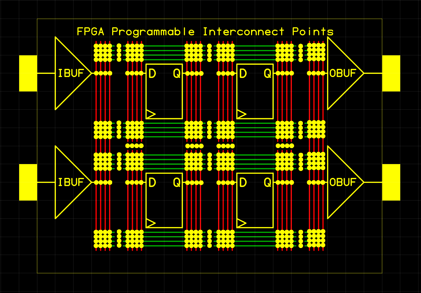
Now just stick this simple LUT in front of each Flip-Flop of an FPGA and some very interesting logic designs can be implemented. Note that Synthesis and Mapping takes care of configuring these LUT memories. Once FPGA configuration has completed, each LUT can be thought of as a fixed Boolean logic gate in function.

Note that actual LUTs in commercial FPGAs are slightly larger, with a few more inputs and outputs. This allows for a single LUT to implement the commonly used circuit of a Full-Adder necessary for creating a binary counter. LUTs can be cascaded into multiple levels of logic. Each level, along with routing, adds propagation delay though. If you have a 200 MHz clock, it’s easy to consume the entire 5 ns clock period between two flip-flops with routing and just a few LUTs between them.

Seems appropriate to close out Part-4 by inferring a 4-bit Full-Adder in Verilog and VHDL and flash the original 4-LEDs in a binary counter fashion. Here is the entire design in Verilog RTL ( including the 1 Hz clock divider ).

and to be completely language neutral, the same RTL design but in VHDL:

And finally, the Verilog netlist exported out of Vivado using the command “write_verilog -force ${design_name}_netlist.v“. The 1 Hz circuit is again removed to keep things clear and simple. The design again has an IBUF and BUFG for the clock tree, 4 OBUFs for driving the external LEDs, 4 Flip-Flops ( FDRE ) and now 4 LUTs. Note that the D(0) LUT has 1 input and 1 output while the D(3) LUT has 4 inputs and 1 output – as expected – to implement a 4bit binary adder.

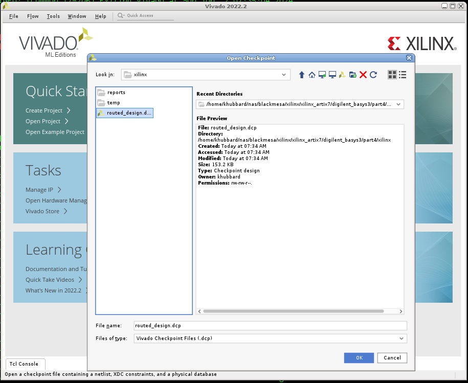
I don’t usually use the Vivado GUI, but I will briefly to close out this Part-4 to illustrate what the fully placed and routed 4-bit binary counter looks like. To do this, I’ll need to add the “write_checkpoint” command to my original “go.tcl” script just after the place and route commands:

[ go.tcl ]
place_design
route_design
write_checkpoint -force routed_design

This will create a file called “routed_design.dcp” that the GUI can then open. From the command line, type “vivado” and then click [ File ], [ Checkpoint ], [ Open ] and selected “routed_design.dcp”.

Once the GUI has loaded the design, you can select the “Leaf Cells” on the left and they will become white highlighted within the floorplan of the FPGA silicon die. The “Leaf Cells” are the gate primitives within the FPGA – the Flip-Flops, LUTs, IO Buffers etc.

Since this FPGA design is mostly empty – I have to Zoom-in a LOT to shows the 4-bit counter design details. Here is a Zoom-in on a single AMD/Xilinx 7-Series “Slice” which contains all 4 flip-flops of the binary counter design. Gone are the simple CLB ( Configurable Logic Block ) days of a 4-input LUT connected to a single flip-flop. You know how an Atom has Protons, Neutrons and Electrons? An AMD/Xilinx 7-Series “Slice” is made up of 8 flip-flops, 4 either 6-input or 5-input LUTs, 3 general purpose 2:1 muxes and a single carry block with some (4) dedicated XORs and 2:1 muxes.

Zoom in a bit more for some more LUT details. What’s fascinating about this, is that I’ve been designing with 7-series parts for a decade now – and I’ve never bothered to know these precise details. That’s the magic of RTL high-level abstraction for FPGA design. I just need to know that there are LUTs between Flops. Having this high-level architecture knowledge prevents me from say inferring a 128bit counter at 300 MHz. The details on how many LUTs and Flops and muxes in a Slice though, that doesn’t influence my day to day decision making at all.

The floorplanner tool by default shows routes ( nets ) in a ratsnest representation. The actual routing is Manhattan-Routing with lots of PIP interconnects along the way.

The routing within a Slice is pretty boring, but highlighting the routing between the D-Flop Q output and the OBUF for driving the LED reveals 14 PIPs spanning a long distance.

Click on the “Routing Resources” button and it switches to a Manhattan-Route view. Funny little circle path it takes towards the OBUF isn’t it? The router had its reasons I’m sure. The great thing is, I don’t have to know the reason why. I just need to know if the route made timing or not.

The important lesson here is that FPGAs have non-infinite metal routing features and routing congestion is often to blame for missing otherwise reasonable timing closure. It is counterintuitive, but I have “saved” many designs in the past by running buses at 4x their necessary rate ( say 400 MHz instead of 100 MHz ) and using this speed advantage to reduce the bus routing width 4x ( say 40 down to 10 ). It’s called time-multiplexing a bus. It’s a 150 year old electrical engineering practice and it’s a critical tool even today for a digital chip designer’s toolbox.

I took this to the extreme with my OSH Sump3 RLE ILA ( here on GitHub ) by having each RLE compression Pod interconnect with the master core controller using only two nets, a MISO+MOSI pair. It’s a distributed logic analyzer requiring minimal global routing resources. My #1 goal with designing Sump3 was to make an ILA that could be added to a “full-up” design and not break the design in the process.

That’s it for Part-4. In Part-5 I show how to simulate the 4-bit counter using ModelSim. For very simple designs ( like the one above ), I just “simulate” the design in my head. Modern FPGAs can have billions of transistors in them though. Once I get beyond a few dozen flip-flops, it’s time to bring in an RTL simulator like Mentor Graphic’s ModelSim.

Since I don’t have Xilinx primitives compiled for my Intel / Altera ModelSim install, I will split the design into a top-level containing Xilinx primitives and a “core” level with inferable RTL for simulation. Excluding IP cores like FIFO, it is customary to separate clock tree and I/O buffers apart from RTL.
EOF

BML FPGA Design Tutorial Part-4ofN

BML FPGA Design Tutorial Part-Intro

Table of Contents:
Part-1 : So what is digital logic design exactly?
Part-2 : Using structural Verilog to make a working FPGA design.
Part-3 : Using RTL Verilog and HDL to infer a working FPGA design.
Part-4 : The magic of LUTs to implement random logic in an FPGA.
Part-5 : Digital Logic Simulation at the RTL level using ModelSim.
Part-6 : Digital Logic Simulation at the RTL level using VivadoSim.

2024.05.18 : I’m Kevin Hubbard, BSEE. It’s hard to believe ( and I constantly pinch myself ), but I’ve been designing with digital logic for 45 years now. I got started as a 1980’s Radio Shack kid, scrounging dollar bills to buy the latest TTL logic chips in DIP packages like the 7400 series ( 7474, 74244, 74245, 74373, 74374, etc ). I built little digital interfaces for my 8bit 6502 Apple ][+ and Z80 TRS-80 Model-1 computers of that era. Everything back then was 1 MHz at 5V. Very forgiving to breadboards, long wires and missing bypass caps ( what are those? ).

My hobbyist passion for electronics steered me to surviving high school and getting a BSEE degree in the early 1990’s from the University of Washington. Zero engineering in the family, but I knew this was what I wanted to do. My career ambitions as a child was either electronics or become a professional LEGO builder. Get this, after graduation companies actually paid me to design digital PCBs, FPGAs and ASICs in the electronics industry. Still pinching myself on that. Also still enjoy building with LEGOs ( without pay ).

30+ years later, my career is not quite sunsetting, but I’ve decided it’s a great time to start sharing a little knowledge learned along my journey in electroincs. I’ve seen things you people wouldn’t believe. 22V10 PALs with only 10 flip-flops costing 10s of dollars transition to Xilinx 4036XLs making the seemingly impossible possible. I watched CMOS Voh/Vih levels drop rapidly from 5V to 1.2V. All those moments will be lost in time, like tears in rain. Time to share some of my knowledge of CMOS digital logic design.

I’m planning a multi-part ( 1ofN ) FPGA design series that starts out super simple ( flashing a “Hello World” LED at 1 Hz ) and gradually move up to a simple VGA graphics “GPU” with an embedded OSH Sump3 ILA logic analyzer for analyzing VGA timing live and interfacing over USB to a Python GUI application running on a PC. I’d like to end with a simple SPI interface to give an RP2040 uC running CircuitPython some cool VGA graphics – TBD. Far too many people think FPGAs are somehow like microcontrollers and designing Verilog/VHDL RTL is somehow the same as software “computer programming”. I wish to enlighten them.

After long and careful consideration, the FPGA Dev Board I selected for this tutorial project is the “BASYS 3” from Digilent. It’s readily available from Amazon ( here ) – making it much easier to acquire than other FPGA dev boards.

So why this board in particular? It has a couple of key features :

  1. Reasonable price at $165. Cheap enough for a person to buy. I’m not really a fan of the $500 to $1,000 boards out there.
  2. Modern (28nm) Artix-7 FPGA that is targetable using the latest free version of AMD / Xilinx Vivado design software.
  3. Built in FTDI USB interface. All of my Python software to FPGA projects use an FTDI FT232 cable, so this interface built in is a key feature.
  4. Simple RGB 4-4-4 analog VGA graphics. Monitors with VGA inputs are still around – so why bother with the TMDS complexity of HDMI graphics? VGA is “good enough” still for some things.
  5. Flexible configuration interface. This board has a unique PIC microcontroller that will read a “top.bit” file from a USB “thumb drive” and configure the FPGA from it.

That last feature closed the deal for me. Simply being able to drop a bitfile onto a USB stick and configure the FPGA from it is a fantastic feature. I develop in a 99% Linux environment and JTAG configuration from Linux has always been problematic. JTAG programming cables can also be expensive ( although this board has an “HS2” compatible one built in as well ). I use low cost 2:1 USB switches like this for sharing a single USB “thumb drive” between multiple host computers ( like a desktop and an oscilloscope ).

Want to join along?
Step-1 : Buy the board.
Step-2 : Download the free Vivado software from AMD / Xilinx website here. I will be using Vivado v2022.2 running on Linux. Which version or platform you use really shouldn’t matter though so long as the Artix7 XC7A35T device is supported.
Step-3 : Start reading along and come back on a regular basis as I post new chapters to the series.

So let’s get started with this FPGA Tutorial from Black Mesa Labs. This quick intro was Part-0.
Part-1, So what is digital logic design exactly?

BML FPGA Design Tutorial Part-Intro

BML FPGA Design Tutorial Part-3ofN

2024.05.19 : I’m Kevin Hubbard, electronics enthusiast who happens to be an Electrical Engineer. In Part-2 of this tutorial I showed how to implement a VERY simple FPGA design of a 4-tap shift-register using a low-level Verilog netlist to instantiate FPGA gate primitives. In Part-3 I will implement the same design using RTL in both Verilog and VHDL HDLs. The entire series “BML FPGA Design Tutorial” begins here.

Structural netlists are ugly. There – I said it. They are hard to write and even harder to read. They are meant for machines, not humans. I can see above that there are four flip-flops in the design (FDSE and FDRE). That said, looking at the schematic is SO much easier to understand. Schematics are horrible though as they take forever to draw and they don’t scale to millions of flip-flops. There must be a better way. And there is – it’s called RTL !

With RTL you can write in a higher level of Verilog ( or VHDL ) which infers the logic elements. Compare the two 100% functionally equivalent flip-flop implementations.

In both cases, the net u0_q will get the binary state of net u3_q on any clk_100m_tree clock edge where the net pulse_1hz is 1. They’re equivalent. Which is easier to read though? Synthesis makes RTL possible. With the magic of Synthesis, a digital logic design can be designed in RTL with very little knowledge of the gate level primitives of the target device. Synthesis automagically infers the FDSE D Flip-Flop given the RTL higher level description of the design.

It gets better though. The original structure design had to instantiate 4 flops with 4 lines of Verilog. With RTL, that can be done in a single line.

The entire original design implemented in RTL suddenly becomes very human readable. Almost enjoyable in fact :

The VHDL design for the same circuit is nearly equivalent:

So what is the difference between VHDL and Verilog RTL? Honestly – very little. VHDL is a strongly typed language where is Verilog is more loose and wild. What does this mean exactly? VHDL takes twice as much typing to accomplish the same results as Verilog. That said, with Verilog, if you don’t know what you’re doing it’s very easy to make mistakes that go unchecked by Synthesis. I like to think I know what I am doing and definitely prefer Verilog.

Back to the 4-tap shift register design, using the Vivado command “write_verilog” – you can have the tool output a IEEE 1364-2001 compliant Verilog HDL file that contains netlist information generated from the input RTL design files. To keep things simple, I removed the pulse_1hz circuit and left only the 4-tap shift register in the design ( running at 100 MHz instead of 1 Hz ). What should be immediately apparent is that the output netlist below from Vivado looks 99% the same as my original Verilog netlist design from Part-2. Everything that I inferred in my high-level RTL design ( IBUFs, OBUFs, BUFGs, FDREs ) all got instantiated by Vivado. Cool huh? What’s also apparent is that FPGAs aren’t magic microcontrollers. They are giant arrays of D Flip-Flops ( and some other stuff to be covered later ).

That’s the end of Part-3 of this tutorial. In Part-4 I explain the magic of FPGA LUTs in implementing combinatorial logic to make fancy things like counters.

EOF

BML FPGA Design Tutorial Part-3ofN

BML FPGA Design Tutorial Part-2ofN


2024.05.19 : I’m Kevin Hubbard, BSEE and Digital Logic Designer.
In Part-1 of this tutorial I attempted to explain the very basics of how an FPGA works and compares with traditional Gate-Arrays as well as standard cell (ASICs and ASSPs ). This is Part-2 of my series “BML FPGA Design Tutorial” which begins here.

My super-simple FPGA example had only 4 Flip-Flops, an input buffer, an output buffer and a whole bunch of metal routing and programmable interconnect points ( PIPs ). In Part-2 of this series I will explain how to implement a simple 4-tap shift register using hardware description language (HDL) at the register-transfer level (RTL) of abstractions.

The end of Part-2 will result in a bitstream file that will configure the PIPs of an AMD/Xilinx Artix-7 FPGA and blink some LEDs on the Digilent BASYS3 development board. It’s a low cost and popular educational board that’s available from Amazon here.

At the beginning of time, “The Ancients” would design FPGAs ( and ASICs ) using schematic entry. It was very labor intensive ( lots of mousing around ) and extremely limiting in terms of how complex a design could scale to. It worked at the time of 22V10s ( 10 Flip-Flops ) and 7032 CPLDs ( 32 Flip-Flops ). Today’s FPGAs like the AMD/Xilinx UltraScale+ have millions of Flip-Flops. Just imagine how much mouse lint “The Ancients” would collect designing a modern FPGA with schematic entry. The graphical schematic entry tools would export the finished design to a netlist file – oftentimes in EDIF format.

Just like how Video Killed the Radio Star, the Verilog HDL ( standardized as IEEE 1364 ) introduced in 1984 killed the EDIF netlist format.

Verilog is heavily influenced by the C programming language in Syntax, but not in function. Verilog might “look like C” but it is not a computer programming language. It is only ever “executed” by software simulators. As a hardware design language it serves three purposes:
1) As a low-level structural netlist ( much like EDIF ).
2) As a behavioral model for simulations ( can model things like propagation delays ).
3) As RTL, a level of abstraction for inferring both combinatorial logic and synchronous logic elements.

Nobody designs FPGAs with schematics anymore, but the tools still support designing with a structural netlist, so my 1st example design in Verilog will do just that using Artix-7 primitive described here. I manually drew a schematic to better explain the Verilog line-by-line.

The design is a four-tap shift register that feeds back on itself. The Q output of each D-Flop drives an LED. Slowed down in time by the clock enable signal pulse_1hz ( circuit not shown ), the result is a BSG Cylon’esq LED that rotates around and around ( but not back and forth like a true Cylon ). Without the “pulse_1hz” circuit, the design would still do its thing, but each LED would be lit for only 10 nS every 40 nS. With the “pulse_1hz” circuit, each LED is lit for 1 Second every 4 Seconds. To build “top.v” without the “pulse_1hz” circuit, just replace “pulse_1hz” with “1”.

Although this “top.v” file is fed into Synthesis – there is no work for Synthesis to actually do. There is nothing to be inferred, only Xilinx primitive gates to be hooked up to each other via wires. The Mapper would also likely pass this netlist right along to Place and Route. My above top.v is intended to be machine readable. Whether it is human readable or not is a matter of opinion.

So what are these gate primitives? They are the physical gates that exist within the FPGA – built at the factory. The simplest are the Input (IBUF) and Output (OBUF) buffers. These IOBs convert the low voltage ( 1.0V ) and low capacitance ( pF or so ) internal nodes within the FPGA to high voltage ( 3.3V ) and high capacitance ( 10 – 100 pF or so ) pins that connect on a circuit board. They do other things too, like provide ESD protection diodes that prevent 1,000s of voltage from an ESD event from destroying internal CMOS gates that are thinner than a bald man’s hairline.

BUFG is the clock tree. Parasitic capacitance of routing, PIPs and gate inputs is a real thing even with CMOS designs. Imagine trying to drive the clock input of 40,000 flip-flops with a single 74HC04 buffer gate. It would not only be incredibly slow, but the current sink would burn up the totem-pole transistors. But now imagine a single 74HC04 buffer driving ten buffers and those ten each driving another ten. After 6 levels of this, you’re driving 100,000 loads with each 74HC04 only seeing 10 loads. That’s a clock tree buffer. They’re also carefully balanced to minimize skew so that all 100,000 loads get their clock edges at approximately the same exact time. Clock trees are very complicated, well thought out and it’s pretty amazing every time I instantiate one with a single line of structural Verilog HDL.

FDSE and FDRE are the D Flip-Flops. They differ only in that the FDSE will “power-up” with a “1” at it’s Q output while the FDREs will have “0”. This forces an input in the circular shift-register ring so that only 1 of the 4 LEDs will be lit at a time.

Now that we have a valid Verilog netlist, it’s time to run it through the AMD/Xilinx Vivado tool to convert the design to an FPGA bitstream. 1st off, we need to create three constraint files:

The 1st of these 3 files is “top_rtl_list.tcl” and it specifies our Verilog design file(s) – in this case, just top.v
The 2nd file “top_timing.xdc” tells Vivado our clock frequency ( 100 MHz, or 10 ns period ). This is important as Vivado needs to know how much routing delay is acceptable to get a signal from the Q output of one Flip-Flop to the D input of the next.
The 3rd file, “top_physical.xdc” tells Vivado about board specific things – like what signal names should go to what pins.

Time to build. I never use the Vivado GUI unless I’m forced to. I generate two files called “go.sh” ( aka go.bat in Windows universe ) and “go.tcl”.

The “go.sh” just launches Vivado in CLI mode and tells it to run “go.tcl”. Tcl is an EDA scripting language invented in 1984 by EDA pioneer John Ousterhout while Professor-ring in Computer Science at UofC Berkeley. Forty years later, Tcl is thoroughly entrenched in the EDA tools industry and it still gets the job done.

The above “go.tcl” specified the FPGA target device and runs the tool suite of Synthesis (+map), Place and Route and outputs a “top.bit” file that can then be dropped onto the USB flash stick in the BASYS3 dev board.

That’s the end of Part-2 of this tutorial. In Part-3 I will implement the same design using high level RTL Verilog which infers gates rather than instantiates them. The Verilog will be human readable – I promise.

EOF

BML FPGA Design Tutorial Part-2ofN

BML FPGA Design Tutorial Part-1ofN

2024.05.18 : So what is digital logic design exactly?

This is Part-1 of my series “BML FPGA Design Tutorial” which begins here.

The D Flip-Flop is the primary building block of digital logic design. A digital logic design deals with binary bits and the simple D Flip-Flop is the keeper of those bits.
From Wikipedia, “The D flip-flop is widely used, and known as a “data” flip-flop. The D flip-flop captures the value of the D-input at a definite portion of the clock cycle (such as the rising edge of the clock). That captured value becomes the Q output. At other times, the output Q does not change. The D flip-flop can be viewed as a memory cell, a zero-order hold, or a delay line.”

Digital logic designs can do truly amazing things. They can implement complex state machines with latency of only a few nanoseconds. They can perform parallel digital signal processing at rates of multiple DVD movies per second. They can electrically interconnect “dumb” semiconductor chips together into a working product. Unlike CPUs, digital logic designs can do everything in parallel ( all tasks at the same time ) rather than sequentially ( one task after the other ).

Ignoring combinatorial logic for now, the simplest thing to build with a bunch of digital D Flops is a shift-register delay line. For that reason, Part-1 and Part-2 of this introductory to FPGAs tutorial will dive into a very simple four-tap shift-register design.

First a little history and comparison of full custom silicon, Gate Arrays and Field Programable Gate Arrays.

At the beginning of time, the Big-Bang of semiconductor electronics happened in 1959 when Robert Noyce at Fairchild Semiconductor invented the very first “Integrated Circuit“. Instead of just a single transistor, Noyce’s IC had multiple transistors. From here fully custom circuits could be built.
Bob Noyce is a Rock God. A giant whose shoulders I stand upon.

For this tutorial, a fully custom silicon chip for a very simple four-tap shift register could be designed and built using CMOS D Flops and it would be both small and fast. Ignoring power, ground and clock – this simple device has only two pins, an input and and output. The logic gates are as close together as possible and metal routing is as short as possible with no wasted silicon. It’s a fully optimized chip design. It would be a little smaller than a 4-bit 74HC93 counter. This smallness and fastness comes at a cost however. That cost is NRE. NRE is both the engineering cost ( in time and salary ) and tooling costs ( reticles or masks ) for producing fully custom silicon. Paying the NRE gets you the smallest ( and cheapest ) silicon. Could there be alternatives to high NREs though?

Enter the Gate-Array in the early 1980’s. With Gate Arrays, a “generic” base wafer design is created that will potentially be used by multiple customers for completely different designs. The NRE for this base wafer can then be amortized down to very little. Think of Gate Arrays like a PCB fully stuffed with 7474 Flip-Flops and 7400-NAND ICs where at the very end, a customer gets to add an additional two routing layers that is unique to their design connecting all the chips. That’s a Gate Array.

Starting with this base wafer, the end customer designs and pays for custom interconnect for this generic array of gates. Typically this only requires custom reticles for one or two metal layers – making gate arrays very affordable. It can lower the price of entry to custom silicon design by 90%. Really. Gate-Arrays were that revolutionary in the 1980’s and 1990’s. I’ve done tape-outs that were the cost of my house and ones that were the cost of my car. I definitely prefer the latter.

This lower Gate-Array NRE does come at a cost. The size of the silicon for this chip is considerably larger than a fully custom design. Why? The gates for the base-wafer are deliberately spaced far apart to allow for varying routing demands of multiple customer designs. Reaching fully gate utilization in a gate-array design is also unlikely. For example, a vendor might offer base-wafers of 10,000 or 20,000 gates. If your design needs 11,000 gates – you pay for the larger 20,000 gate base-wafer area. The same goes for package size and pin counts. So although your NRE may be 10% of full-custom, your piece price may be 200% or 300%. So even though the NRE may be nearly free, nothing is ever free. Also, everything ends Tony.

By the early 1990’s, LSI Logic ASICs pretty much killed the Gate-Array industry. While this slow death was happening a new technology called the FPGA ( Field Programmable Gate Array ) entered the market. In 1984, a guy named Ross Freeman came up with this radical idea of making a gate array that was fully programmable in-field rather than metal masked configured at the foundry. With his radical new idea began Xilinx ( now part of AMD ).

Just like a traditional Gate-Array, an FPGA has a base-wafer like design with gates that are not connected to each other and are spaced far apart. What differs is that the FPGA is already fully metalized with a giant matrix of metal routing that allows any flip-flop to connect to any other flip-flop across the chip. It’s a bit like a freeway system where all the on and off ramps are draw-bridges that become either open or closed depending on the end user’s design.

These connections are done just after powerup using pass-transistors (switches) called “Programmable Interconnect Points” or PIPs. It’s really a crazy concept. An off-chip EEPROM stores dozens of PIP configuration bits for each user accessible flip-flop in an FPGA. On powerup, the EEPROM contents are fed into a giant shift-register of non-user flip-flops which then either open or close each PIP. This configuration can take 100’s of milliseconds – which is forever in the digital realm.

At a bitstream level, designing an FPGA is akin to designing a printed circuit board. The designer is deciding how to connect things electrically but within the chip itself. Thankfully, with millions to billions of PIPs to decide upon, today’s EDA tools offer higher levels of abstraction ( RTL ) which I will start to explain in Part-2.

My example super-simple FPGA below has only 4 user flip-flops, but more than 400 PIPs. These PIPs are not drawn to scale ( they are much larger than a single silicon via ). The Artix-7 XC7A35T FPGA used later in this tutorial has 40,000 flip-flops and requires 1,600,000 PIP configuration bits. Thankfully flash memory is dirt cheap these days ( it wasn’t in the 1980’s and 1990’s ). A $100 FPGA might have an external flash EEPROM costing only $1 or $2. Ross Freeman’s brilliance wasn’t skating to the puck, but skating to where the puck was going.

Not counting diffused IP like multipliers and RAMS, the actual overhead for an FPGA versus custom silicon is about 10x. This means a purely digital logic design will consume about 10x the CMOS area in an FPGA as it would in an ASIC. FPGAs cost more than custom silicon, but custom silicon NREs are now more than $1 million USD – so there’s a market for them for low volume designs.
Would a company be better off spending $1M NRE and $10 per ASIC or $0 NRE and $100 per FPGA?
Ay, there’s the rub.

The original 4-tap shift register design implemented in the above FPGA would look like this:

What is noteworthy is that the vast majority of the metal routing channels go unused. Very few PIPs are actually closed. They are all still consuming die area and must be paid for both in wafer test time and silicon area. The routing is also quite slow compared to full custom silicon. Not only are the routes much longer ( die is 10x the size, so more capacitance ) but each PIP also has parasitic resistance and capacitance relative to near-0 of metal vias in a fully custom ASIC, ASSP or even Gate-Array design. These PIP connected long Manhattan routes take nanoseconds instead of 100’s of picoseconds. Early generation FPGAs at 350nm were slow, running at only 20 to 40 MHz. Today’s 14nm FPGAs run comfortably at 200 to 300 MHz for many designs.

So what does this all mean? FPGAs will never compete with full custom silicon for things like 3 GHz CPUs and GPUs. For many applications though, 300 MHz is “good enough” and million dollar NREs are just way too much.

This ends Part-1 of the BML FPGA Tutorial. In Part-2 I show how to implement this simple 4-tap shift-register in structural Verilog and then Synthesize, Map and Place and Route into an AMD/Xilinx Artix-7 FPGA bitstream and flash some LEDs on the Digilent BASYS3 board.

Future Part-3 of this tutorial will explain Inferring gates using Verilog-RTL and how FPGA LUTs are used to implement generic combinatorial logic. I hope that you enjoyed this introduction to FPGAs and found it informative.
EOF

BML FPGA Design Tutorial Part-1ofN